Method for mounting an electronic component on a substrate

Inactive Publication Date: 2012-03-06
NAGRAVISION SA
View PDF23 Cites 6 Cited by
  • Summary
  • Abstract
  • Description
  • Claims
  • Application Information

AI Technical Summary

Benefits of technology

[0013]The aim of this invention is to avoid the drawbacks described above, namely to increase reliability and quality of the electric connection between the electronic component or components and the substrate conductive tracks while reducing the manufacturing costs of the transponder.
[0023]The advantage of mounting the component according to this method resides in the fact that the contact between the component and the circuit conductor is maintained when the transponder is bent or twisted. In fact, the internal forces appearing at the level of connection tend to make the contacts slide one on the other without producing any breakage as in the case of a welded or anchored connection. Repeated stresses exerted on the transponder cause a “self-cleaning” effect on the conductors by rubbing their surfaces together. Therefore, the performance of the connection as well as its reliability and its electric conductivity are greatly improved.

Problems solved by technology

The transponders whose components are assembled according to the known processes described above present a disadvantage at the level of quality and reliability of the connection between the component and conductors.
Despite the protection of the components by coating or lamination of an insulating film, the connections of the components are subjected to internal traction and compression causing their breakage when the transponder is deformed.
This phenomenon is further increased during repetitive deformations leading to the strain of the connection that will finally break after a few flexions or torsions suffered by the transponder.

Method used


Image

  • Method for mounting an electronic component on a substrate
  • Method for mounting an electronic component on a substrate
  • Method for mounting an electronic component on a substrate

Examples


Embodiment Construction

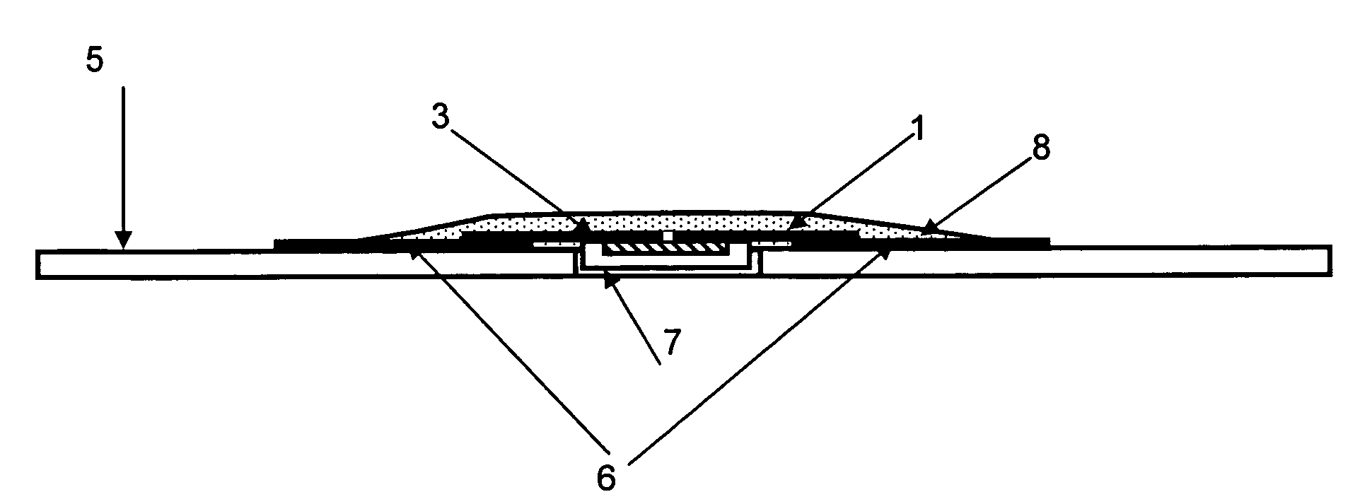
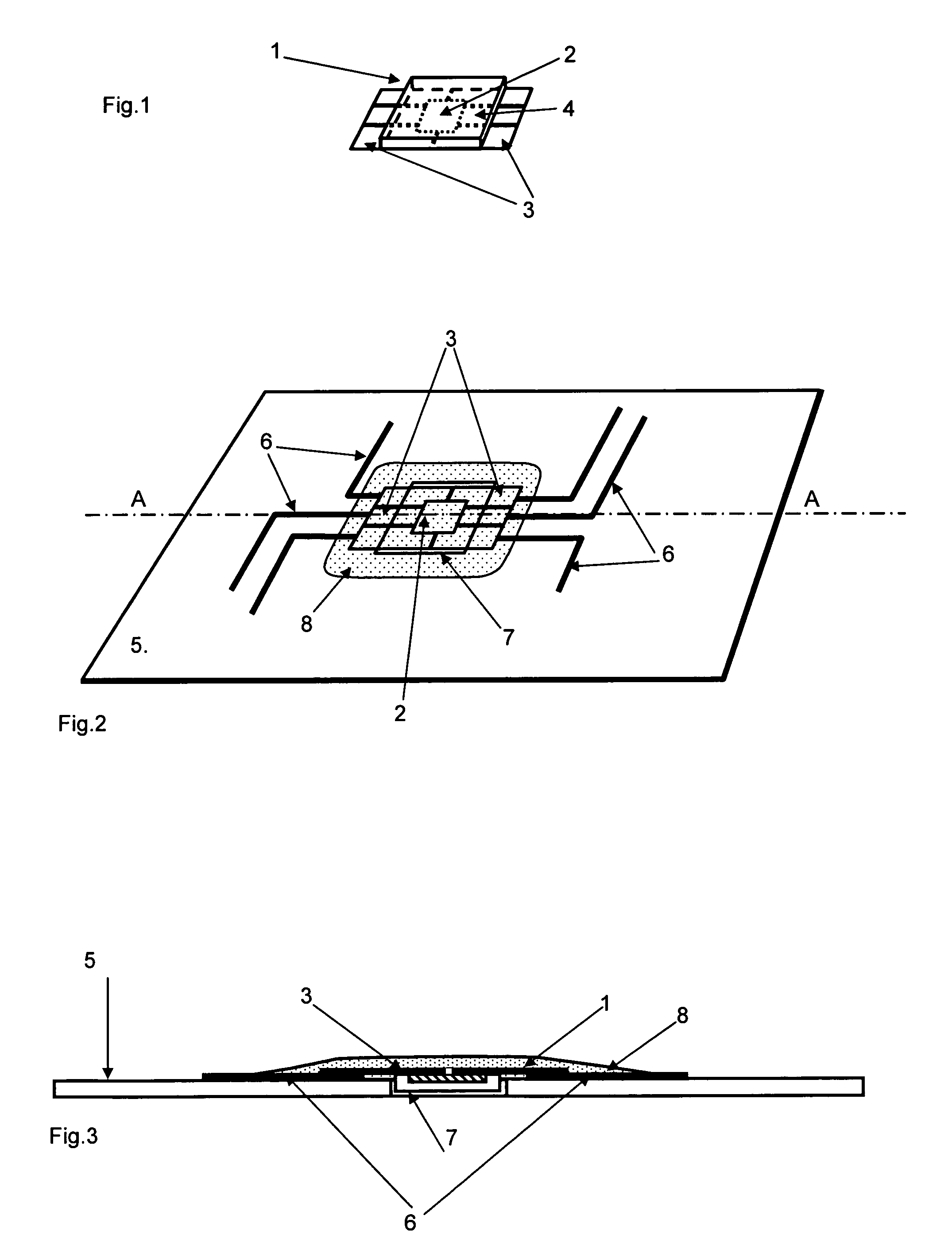
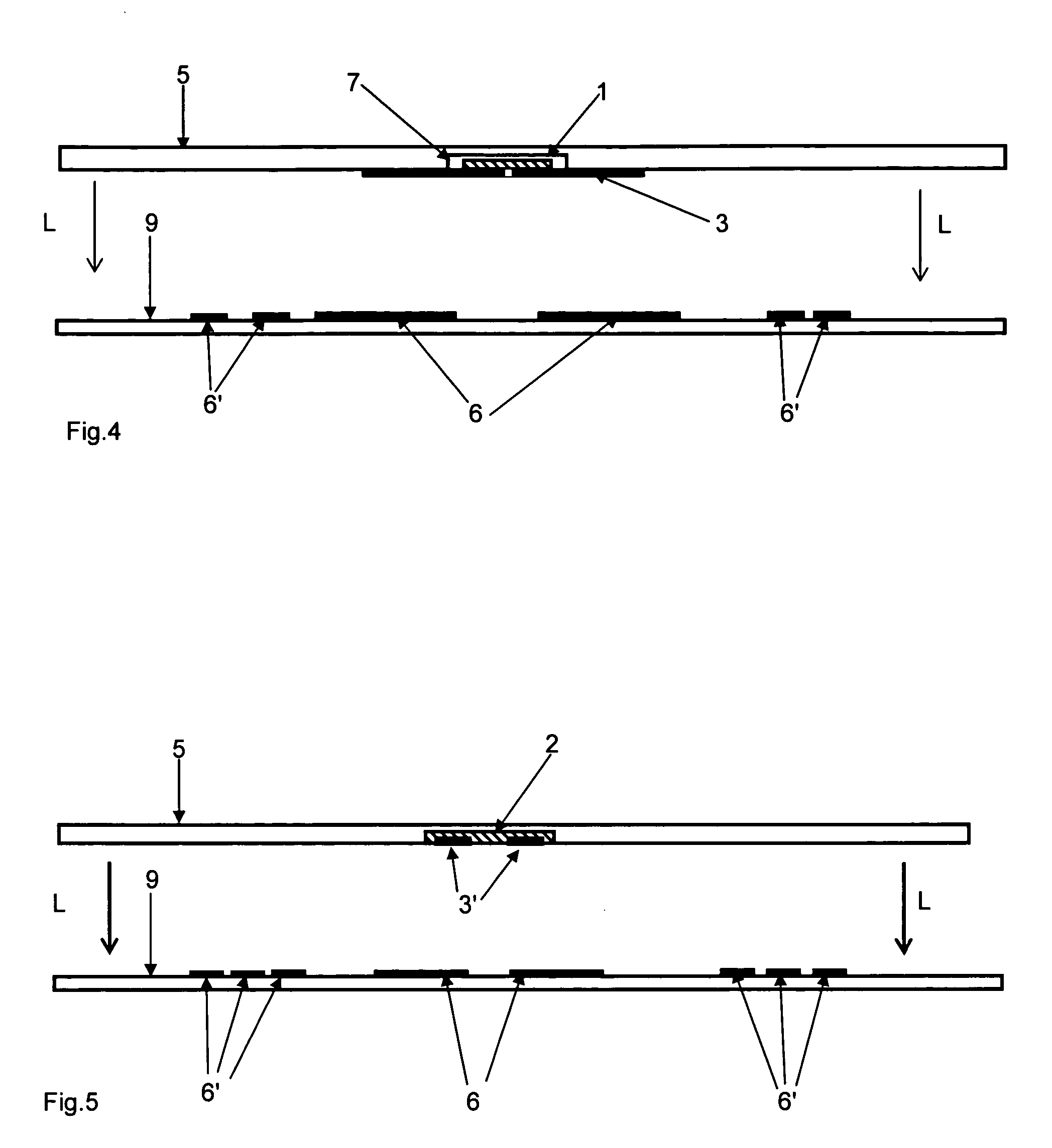
[0030]The component (1) in FIG. 1 forming an electronic module includes a chip (2) protected by coating (4) in insulating material such as an epoxy resin. The chip contacts are connected to contact areas (3) formed inside a tinned copper conductive sheet, for example, forming the “lead frame”.

[0031]FIG. 2 and the section according to the illustrated axis A-A in FIG. 3 show an example of a transponder that includes a thin substrate (5) that can be deformed on which the component (1) in FIG. 1 is placed. The upper surface of said substrate includes tracks or conductive areas (6) engraved, glued or printed by silk-screening, for example. The coated part (4) of the component (1) is inserted into a cavity (7) made up of milling or a window cut into the substrate in order to minimize the final thickness of the transponder. The conductive tracks (6) of the substrate are in contact with the component conductive areas (3) only by means of pressure without using welding or conductive glue. Th...


PUM

PropertyMeasurementUnit
Pressureaaaaaaaaaa
Electrical conductoraaaaaaaaaa
aaaaaaaaaa

Abstract

This invention proposes a manufacturing process for a transponder in the form of a card or a label able to resist to flexions or twisting without interrupting the connections of the electronic components. The process of assembling at least one electronic component including sensibly flat conductive areas that are connected to conductive tracks placed on the surface of a generally flat substrate comprises the steps of placing the substrate on a work surface, the face including conductive tracks being oriented upwards, placing the electronic component into a cavity of the substrate situated in a zone including the conductive tracks, the conductive areas of the component coming into contact with the corresponding tracks of the substrate and applying a layer of insulating material which extends at once on the electronic component and at least on a substrate zone surrounding said component. This process implies that the contact between the conductive areas of the electronic component and the conductive tracks of the substrate realizes an electric connection ensured by the pressure of application of the insulating material layer on the electronic component.

Description

[0001]This application is the national phase under 35 U.S.C. §371 of PCT International Application No. PCT / IB2004 / 050645, which has an international filing date of May 12, 2004, which designated the United States of America and which claims priority on Switzerland Patent Application CH0832 / 03, filed May 13, 2003, the entire contents of which are hereby incorporated herein by reference.FIELD OF THE INVENTION[0002]This invention relates to an assembly process of an electronic component on an insulating support called a substrate that includes a plurality of conductive tracks. This process can be applied during the manufacturing of transponders in the form of a card or an electronic label which thickness is generally low.[0003]Electronic label is understood to mean an assembly comprising at least one insulating support, an antenna and an electronic component, usually a chip. The card or electronic label made using the process according to the invention is found in numerous applications...

Claims


Application Information

Patent Timeline
IPC IPC(8): G06K5/00G06K19/06B23K1/00G06K19/077H05K1/18H05K3/28H05K3/32
CPCB23K1/0008G06K19/07728G06K19/07745G06K19/07749H05K3/325B23K2201/40H05K1/182H05K3/284H01L2924/0002H05K2201/10727H05K2203/1311H01L2924/00B23K2101/40H05K13/00H05K13/04
Inventor DROZ, FRANCOIS
Owner NAGRAVISION SA
Why Eureka
Try Eureka