Semiconductor device including MISFETs having different threshold voltages

a technology of semiconductor devices and misfets, which is applied in the direction of semiconductor devices, radio frequency controlled devices, electrical apparatus, etc., can solve the problems of unresolved above-mentioned problems, and achieve the effect of high precision and high performan

Active Publication Date: 2012-03-06
PANNOVA SEMIC
View PDF16 Cites 7 Cited by
  • Summary
  • Abstract
  • Description
  • Claims
  • Application Information

AI Technical Summary

Benefits of technology

[0014]However, in this case, since the channel region of the high threshold voltage MIS transistor has a relatively high impurity concentration, carriers collide with conductivity type impurities contained in the channel region to be scattered during an operation of the semiconductor device, so that the mobility of the carriers is decreased and therefore the drive force is reduced in the high threshold voltage MIS transistor.
[0057]As described above, according to the semiconductor device of the present invention and its fabrication method, by adjusting the film thicknesses of the conductive portions (or the conductive material of the conductive portions) provided on and contacting the first and second gate insulating films included in the first and second MIS transistors, the effective work function of the second MIS transistor is controlled to be higher than the effective work function of the first MIS transistor. Therefore, it is possible to achieve a semiconductor device comprising first and second MIS transistors having the same conductivity type, in which the first and second MIS transistors can be caused to have different threshold voltages with high precision and have high performance.

Problems solved by technology

Therefore, the aforementioned problem is still not solved.

Method used


Image

  • Semiconductor device including MISFETs having different threshold voltages
  • Semiconductor device including MISFETs having different threshold voltages
  • Semiconductor device including MISFETs having different threshold voltages

Examples


first embodiment

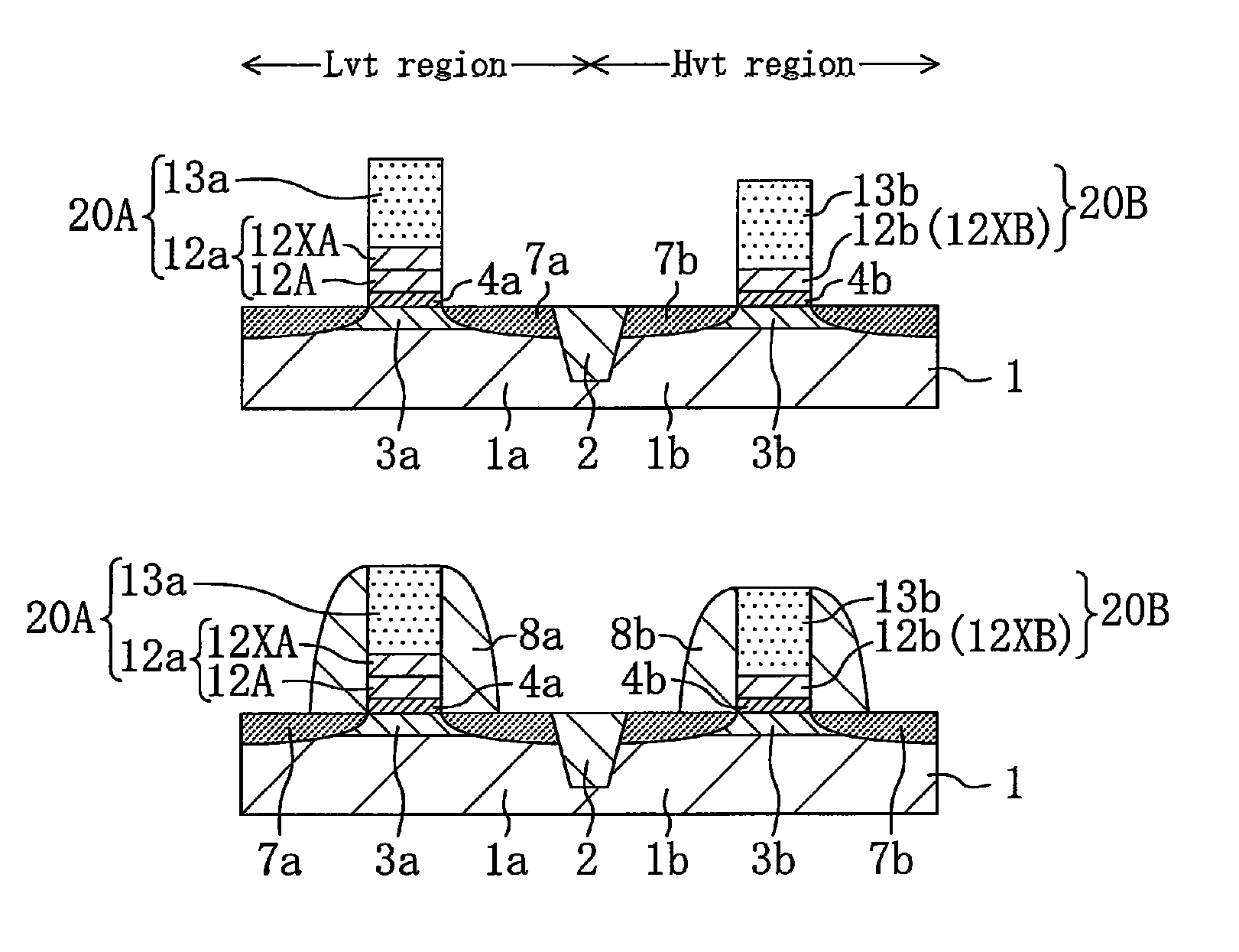
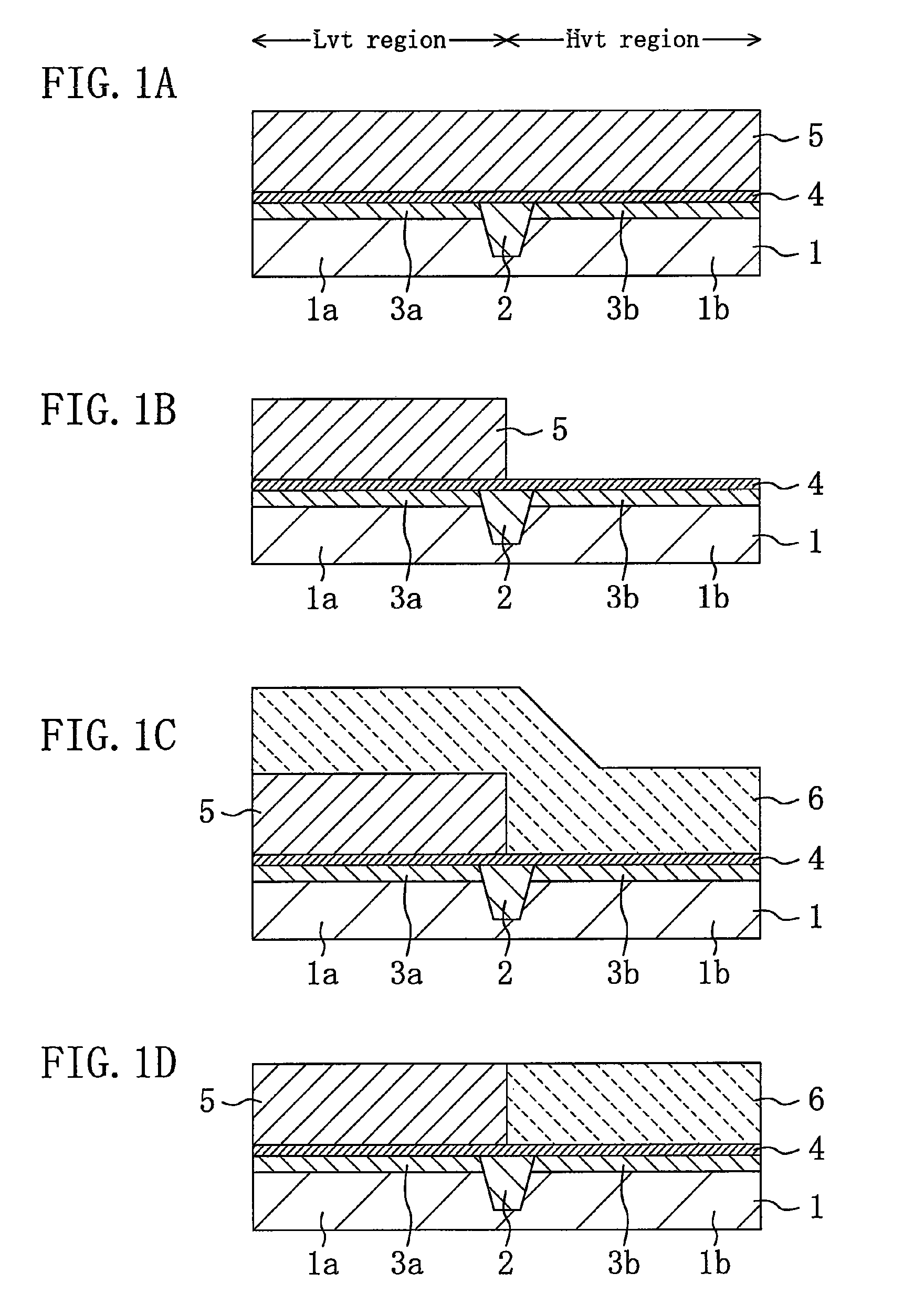
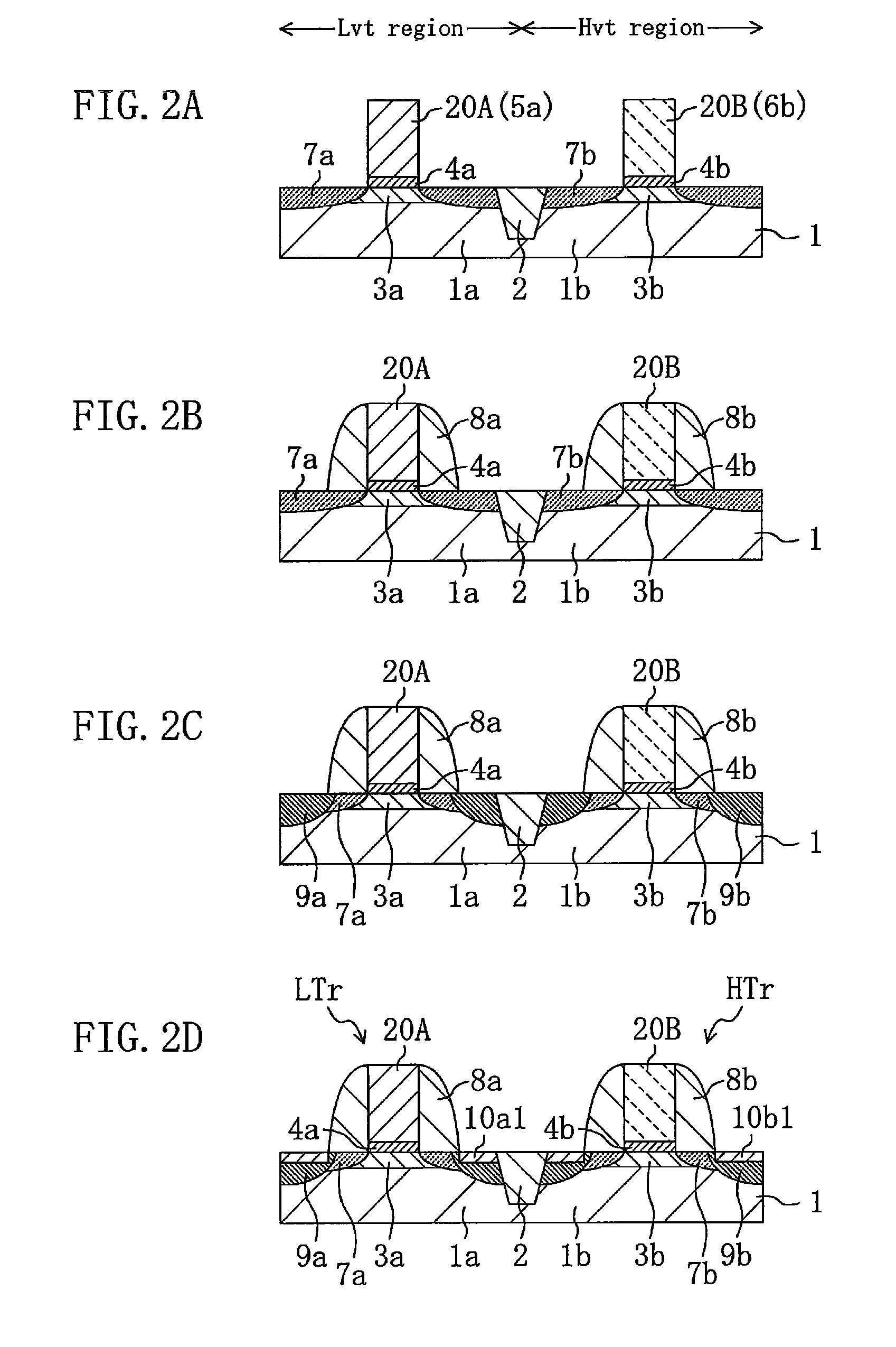
[0076]Hereinafter, a method for fabricating a semiconductor device according to a first embodiment of the present invention will be described with reference to FIGS. 1A to 1D and 2A to 2D, illustrating a specific example in which p-type MIS transistors are employed as MIS transistors having different threshold voltages. FIGS. 1A to 1D and 2A to 2D are cross-sectional views showing major steps of the fabrication method of the semiconductor device according to the first embodiment of the present invention in an order in which the device is fabricated. Note that, in this embodiment, a Lvt region is a region in which a p-type MIS transistor having a relatively low threshold voltage (hereinafter referred to as a “low threshold transistor”) is formed, and a Hvt region is a region in which a p-type MIS transistor having a relatively high threshold voltage (hereinafter referred to as a “high threshold transistor”) is formed.

[0077]Initially, as shown in FIG. 1A, for example, by using a Shall...

second embodiment

[0108]Hereinafter, a method for fabricating a semiconductor device according to a second embodiment of the present invention will be described with reference to FIGS. 3A to 3D and 4A to 4D, illustrating a specific example in which p-type MIS transistors are employed as MIS transistors having different threshold voltages. FIGS. 3A to 3D and 4A to 4D are cross-sectional views showing major steps of the fabrication method of the semiconductor device according to the second embodiment of the present invention in an order in which the device is fabricated. Note that, in FIGS. 3A to 4D, the same parts as those of the first embodiment are indicated by the same reference symbols as those shown in FIGS. 1A to 2D and will not be repeatedly described. Note that, in this embodiment, a Lvt region is a region in which a low-threshold MIS transistor is formed, and a Hvt region is a region in which a high-threshold MIS transistor is formed.

[0109]Initially, a step similar to that of the first embodi...

third embodiment

[0134]Hereinafter, a method for fabricating a semiconductor device according to a third embodiment of the present invention will be described with reference to FIGS. 5A to 5D, illustrating a specific example in which p-type MIS transistors are employed as MIS transistors having different threshold voltages. FIGS. 5A to 5D are cross-sectional views showing major steps of the fabrication method of the semiconductor device according to the third embodiment of the present invention in an order in which the device is fabricated. Note that, in FIGS. 5A to 5D, the same parts as those of the first embodiment or the second embodiment are indicated by the same reference symbols as those shown in FIGS. 1A to 2D in the first embodiment or those shown in FIGS. 3A to 4D in the second embodiment, and will not be repeatedly described. Note that, in this embodiment, a Lvt region is a region in which a low-threshold MIS transistor is formed, and a Hvt region is a region in which a high-threshold MIS ...


PUM


Abstract

A semiconductor device includes a first MIS transistor, and a second MIS transistor having a threshold voltage higher than that of the first MIS transistor. The first MIS transistor includes a first gate insulating film made of a high-k insulating film formed on a first channel region, and a first gate electrode having a first conductive portion provided on and contacting the first gate insulating film and a second conductive portion. The second MIS transistor includes a second gate insulating film made of the high-k insulating film formed on a second channel region, and a second gate electrode having a third conductive portion provided on and contacting the second gate insulating film and a fourth conductive portion. The third conductive portion has a film thickness smaller than that of the first conductive portion, and is made of the same composition material as that of the first conductive portion.

Description

CROSS REFERENCE TO RELATED APPLICATIONS[0001]This Non-provisional application claims priority under 35 U.S.C. §119(a) on Patent Application No. 2008-014818 filed in Japan on Jan. 25, 2008, the entire contents of which are hereby incorporated by reference.BACKGROUND OF THE INVENTION[0002]1. Field of the Invention[0003]The present invention relates to a semiconductor device and its fabrication method. More particularly, the present invention relates to a semiconductor device comprising multi-Vt MISFETs (Metal Insulator Semiconductor Field Effect Transistors) having different threshold voltages, and its fabrication method.[0004]2. Description of the Related Art[0005]In recent years, in order to achieve a semiconductor integrated circuit device that simultaneously has high performance and low power consumption, a multi-Vt process is commonly used in which MISFETs (hereinafter referred to as “MIS transistors”) that have the same conductivity type and different threshold voltages are embe...

Claims


Application Information

Patent Timeline
Patent Type & Authority Patents(United States)
IPC IPC(8): H01L21/336
CPCH01L21/82345H01L29/105H01L29/517H01L21/26513Y10S257/901
Inventor HIRASE, JUNJI
Owner PANNOVA SEMIC
Why Eureka
Try Eureka