
Method for manufacturing a phase change memory device with pillar bottom electrode

a memory device and bottom electrode technology, applied in semiconductor devices, digital storage, instruments, etc., can solve the problems of reliability and yield problems, cell in the array permanently disconnected from the access circuit, and the underlying access circuitry at the bottom of very small vias is difficult to form reliable contact, etc., to improve the operation characteristics of the memory cell, improve the electrical connection to the pillar, and improve the current density

Active Publication Date: 2012-03-20
GLOBALFOUNDRIES US INC +2
View PDF207 Cites 35 Cited by
  • Summary
  • Abstract
  • Description
  • Claims
  • Application Information

AI Technical Summary

Benefits of technology

The patent describes a method for manufacturing a mushroom-cell type phase change memory with superior uniformity of critical dimensions and electrical connection. The process involves depositing a layer of bottom electrode material over a substrate with access circuitry, making reliable electrical contact with the access circuitry. The electrode material is then patterned to form electrode pillars on the conductive contacts. A layer of dielectric material is deposited over the electrode pillars and the contact surface, followed by a layer of programmable resistive material and a layer of top electrode material. The process also includes forming pads for individual memory cells, patterning the programmable resistive material and conductor layer, and etching the electrode material to form the pillars. The patent also describes variations of the process, such as using a multilayer stack for the bottom electrode material, etching recesses in the electrode pillars, and tapering the electrode pillars. The technical effects of the patent include improved operational characteristics of the memory cell and mechanical stability during manufacturing.

Problems solved by technology

Although this technique is suitable for forming very small bottom electrode structures using plugs in vias, it has proved to suffer reliability and yield issues.
For example, as described by Ahn et al., it has proven difficult to form reliable contact with the underlying access circuitry at the bottom of very small vias.
This results in some cells in the array permanently disconnected from the access circuits.
Furthermore, Ahn et al. have related that it is difficult to ensure in the plug-in-via process that the areas of the exposed tops of the plug electrodes are uniform after the planarizing step across a large array of such cells.
This problem is exacerbated by the techniques used in attempts to successfully fill the vias, including depositing thin films and anisotropic etching of the thin films to form sidewall spacers with the vias.
Because it is difficult to planarize the resulting structure uniformly across an entire array within tolerances sufficient to avoid this expanding top end, the etch back will not remove the expanded top end completely for all of the cells and results in a significant variation in size of the exposed top surface of the bottom electrode plugs.
Yet another problem arises in the formation of plug in via electrodes, because of the difficulty of uniformly filling vias.
In particular, due to the dynamics of thin film deposition within small holes, the plug that results may include a void where the top of the via closes off before it has been completely filled below.
Such holes cause problems with successful formation of a layer of phase change material over the electrode.

Method used


Image

  • Method for manufacturing a phase change memory device with pillar bottom electrode
  • Method for manufacturing a phase change memory device with pillar bottom electrode
  • Method for manufacturing a phase change memory device with pillar bottom electrode

Examples


Embodiment Construction

[0030]The following detailed description is made with reference to the figures. Those of ordinary skill in the art will recognize a variety of equivalent variations on the description that follows.

[0031]With regard to directional descriptions herein, the orientation of the drawings establish their respective frames of reference, with “up,”“down,”“left” and “right” referring to directions shown on the respective drawings. Similarly, “thickness” refers to a vertical dimension and “width” to the horizontal. These directions have no application to orientation of the circuits in operation or otherwise, as will be understood by those in the art.

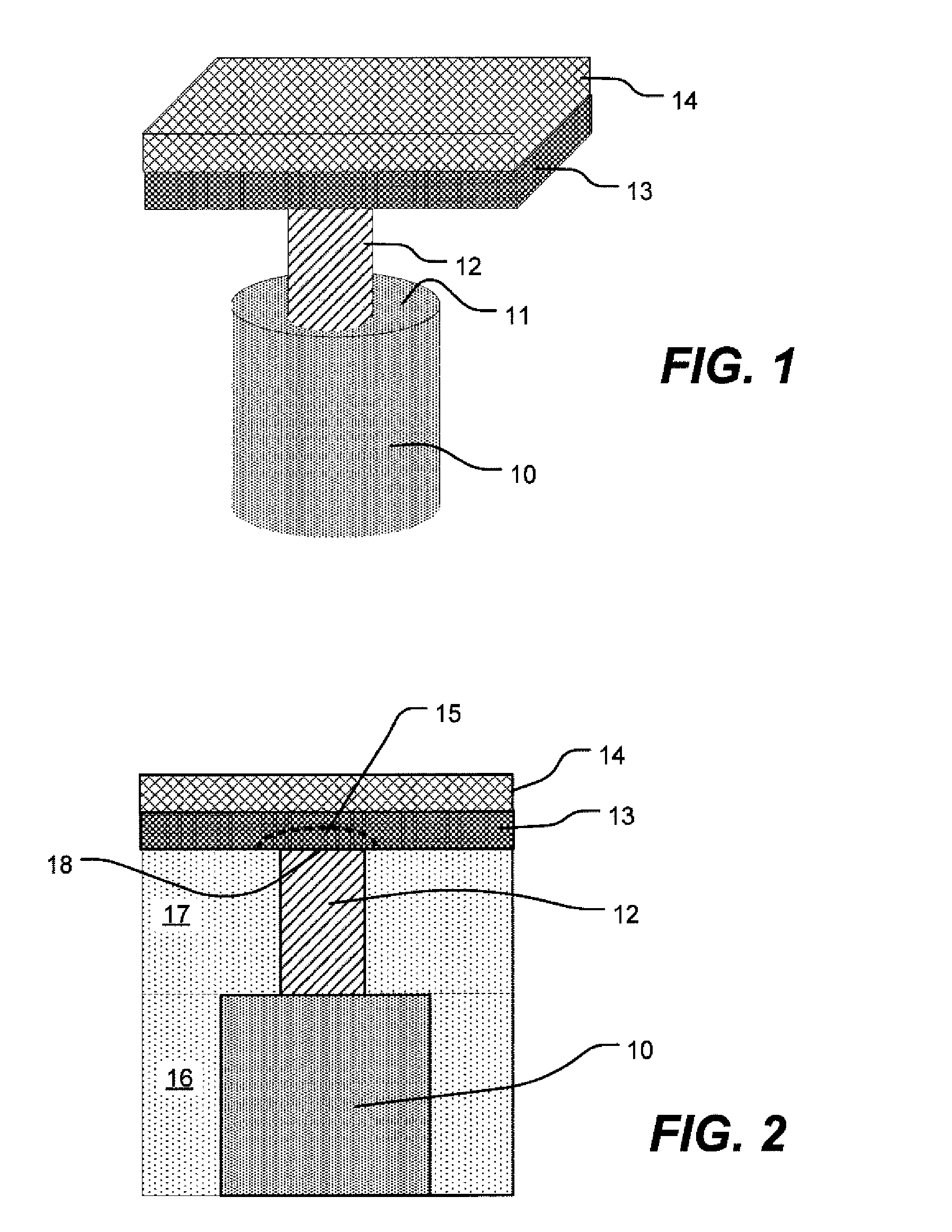
[0032]FIG. 1 provides a prospective view of the basic structure of a phase change memory cell manufactured as described herein with dielectric fill material removed from the drawing. The memory cell is formed on a contact 10 having a contact surface 11. Contact 10 comprises a “plug” extending through an inter-layer dielectric to underlying access c...


PUM


Abstract

A method for manufacturing a mushroom-cell type phase change memory is based upon manufacturing a pillar of bottom electrode material upon a substrate including an array of conductive contacts in electrical communication with access circuitry. A layer of electrode material is deposited making reliable electrical contact with the array of conductive contacts. Electrode material is etched to form a pattern of electrode pillars on corresponding conductive contacts. Next, a dielectric material is deposited over the pattern and planarized to provide an electrode surface exposing top surfaces of the electrode pillars. Next, a layer of programmable resistive material, such as a chalcogenide or other phase change material, is deposited, followed by deposition of a layer of a top electrode material. A device including bottom electrode pillars with larger bottom surfaces than top surfaces is described.

Description

REFERENCE TO RELATED APPLICATION[0001]This application claims the benefit of U.S. Provisional Patent Application No. 60 / 889,415, filed 12 Feb. 2007 by the same co-inventors, entitled Method for Manufacturing a Phase Change Memory Device with Pillar Bottom Electrode, which is incorporated by reference herein.PARTIES TO A JOINT RESEARCH AGREEMENT[0002]International Business Machines Corporation, a New York corporation; Macronix International Corporation, a Taiwan corporation; and Infineon Technologies A.G., a German corporation, are parties to a Joint Research Agreement.BACKGROUND OF THE INVENTION[0003]1. Field of the Invention[0004]The present invention relates to methods for manufacturing high density memory devices based on phase change based memory materials, including chalcogenide based materials and other materials, and most particularly to methods for manufacturing a phase change memory element with a pillar-shaped bottom electrode.[0005]2. Description of Related Art[0006]Phase...

Claims


Application Information

Patent Timeline
Patent Type & Authority Patents(United States)
IPC IPC(8): H01L45/00
CPCG11C13/0004H01L27/2436H01L45/04H01L45/06H01L45/1233H01L45/126H01L45/1675H01L45/144H01L45/146H01L45/147H01L45/148H01L45/1625H01L45/1641H01L45/14H10B63/30H10N70/20H10N70/8413H10N70/881H10N70/8836H10N70/231H10N70/884H10N70/026H10N70/041H10N70/8828H10N70/8833H10N70/063H10N70/826
Inventor LUNG, HSIANG LANCHEN, CHIEH FANGCHEN, YI CHOUCHEN, SHIH HUNGLAM, CHUNG HONJOSEPH, ERIC ANDREWSCHROTT, ALEJANDRO GABRIELBREITWISCH, MATTHEW J.BURR, GEOFFREY WILLIAMHAPP, THOMAS D.PHILIPP, JAN BORIS
Owner GLOBALFOUNDRIES US INC
Learn More