Check patentability & draft patents in minutes with Patsnap Eureka AI!

Semiconductor device

a technology of semiconductors and devices, applied in the direction of pulse manipulation, instant pulse delivery arrangements, pulse techniques, etc., can solve the problems of large voltage difference, inability to detect the voltage of every cell with high precision, and difficult to detect the voltage of batteries with high precision, so as to facilitate the detection of the voltage of each cell, reduce the error caused by voltage drop, and reduce the resistance

Inactive Publication Date: 2012-04-03
FUJI ELECTRIC CO LTD
View PDF3 Cites 2 Cited by
  • Summary
  • Abstract
  • Description
  • Claims
  • Application Information

AI Technical Summary

Benefits of technology

Enables precise detection of each cell voltage in a battery, improving charging safety and accuracy by reducing errors associated with voltage division, and facilitating high-precision voltage monitoring across multiple cells.

Problems solved by technology

However, a large voltage difference is caused between a battery voltage and a reference voltage level, to which the battery voltage is lowered, in the voltage detecting circuit section in a charging control IC for a battery including many cells.
The large voltage difference makes it hard to detect the battery voltage with high precision.
Since only one reference voltage circuit is included, it is impossible to detect the voltage of every cell.

Method used


Image

  • Semiconductor device
  • Semiconductor device
  • Semiconductor device

Examples


first embodiment

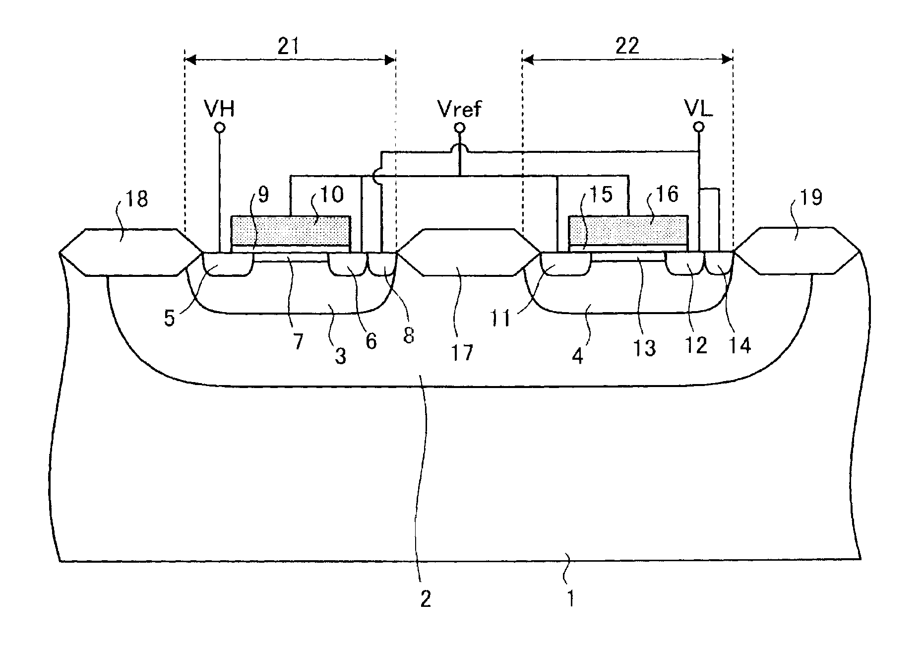
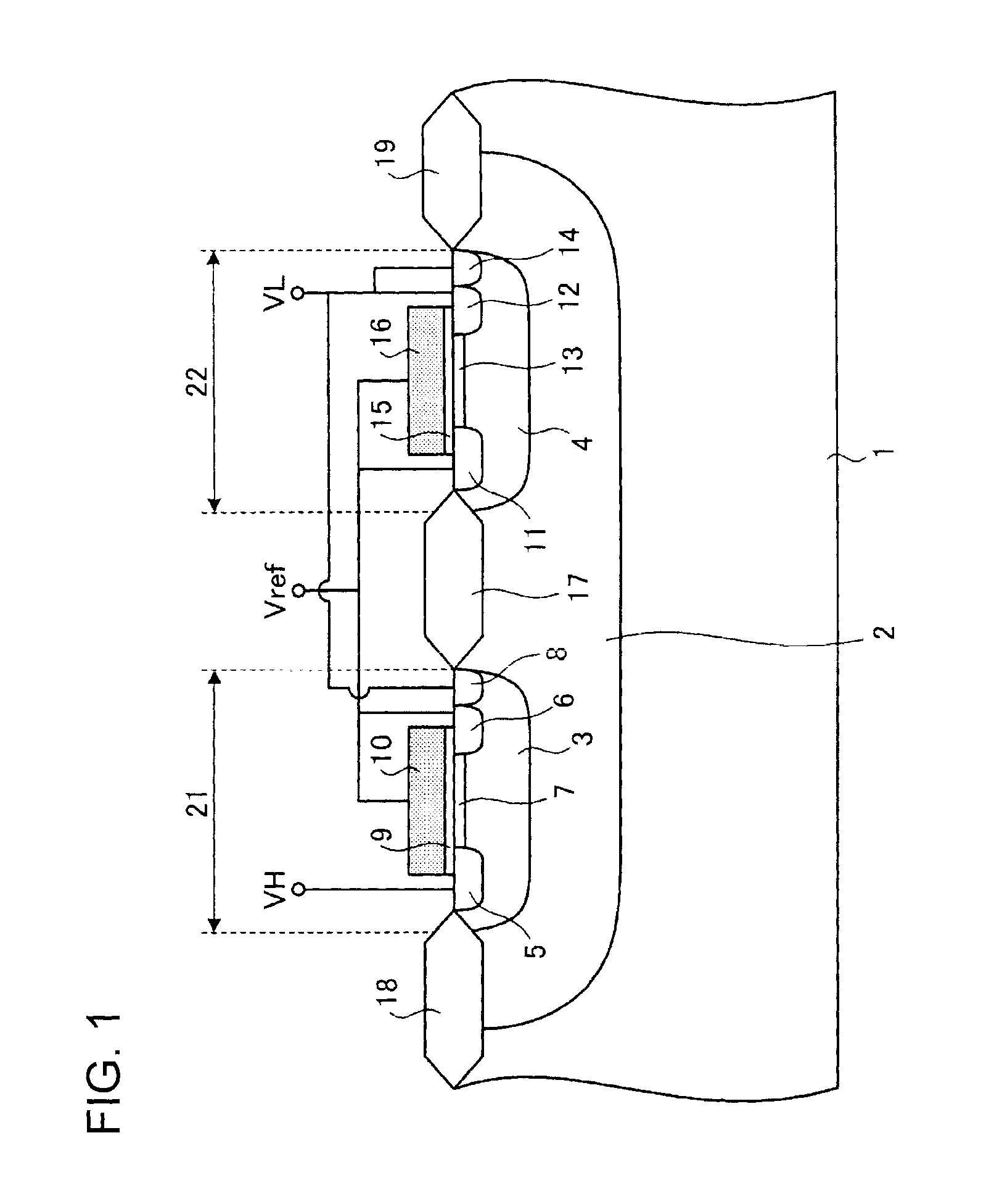
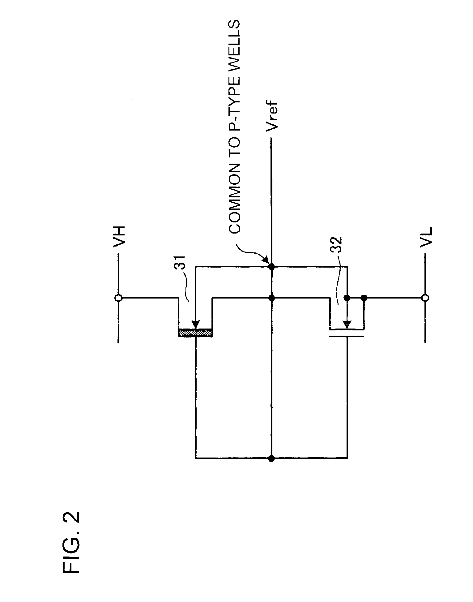
[0033]Now the method for manufacturing a MOS reference voltage circuit according to the invention will be described below. First, n-type well layer 2 is formed in the surface portion of p-type substrate 1. Then, field oxide films 17, 18 and19 are formed. In the surface portion of n-type well layer 2, p-type well layers 3 and 4 are formed. Then, n−-type depletion layer 7 is formed in the surface portion of p-type well layer 3. Depletion layer 7 is doped, for example, with phosphorus (P31). Then, gate oxide film 9 of, for example, 170□ in thickness is formed on n−-type depletion layer 7. Further, gate electrode 10 is deposited on gate oxide film 9.

[0034]In p-type well layer 4, p−-type channel layer 13 is formed. Then, gate oxide film 15 of, for example, 170 Å in thickness is formed on p−-type channel layer 13. Further, gate electrode 16 is deposited on gate oxide film 15.

[0035]Shielding masks are formed on the portions of p-type well layers 3 and 4, in which any n+-type layer will not...

second embodiment

[0042]The semiconductor device facilitates detecting a voltage very precisely when it is required for the semiconductor device to exhibit a breakdown voltage of around 10 V.

[0043]FIG. 5 is a cross sectional view of a semiconductor device according to a third embodiment of the invention. The semiconductor device according to the third embodiment is different from the semiconductor devices according to the first and second embodiments in that the semiconductor device according to the third embodiment is manufactured using an epitaxial substrate. As shown in FIG. 5, the epitaxial substrate includes n-type buried layer 71 on p-type substrate 1, and p-type epitaxial layer 72 laminated on n-type buried layer 71. Epitaxial layer 72 works as a floating layer. In the surface portion of p-type epitaxial layer 72, p-type well layer 73 is formed. In the surface portion of p-type well layer 73, depletion-type NMOSFET 101 and enhancement-type NMOSFET 102 are formed such that depletion-type NMOSF...


PUM


Abstract

A semiconductor device can output a reference voltage for an arbitrary potential and can detect the voltage of each cell in a battery including multiple cells very precisely. The device includes a depletion-type MOSFET 21 and an enhancement type MOSFET 22, and has a floating structure that isolates depletion-type MOSFET 21 and enhancement type MOSFET 22 from a ground terminal. The depletion-type MOSFET 21 and enhancement type MOSFET 22 are connected in series to each other, wherein the depletion-type MOSFET 21 is connected to high-potential-side terminal and the enhancement type MOSFET 22 is connected to low-potential-side terminal. The semiconductor device having the configuration described above is disposed in a voltage detecting circuit section in a control IC for a battery including multiple cells.

Description

BACKGROUND[0001]The present invention relates to a semiconductor device. Specifically, the invention relates to a semiconductor device for outputting a reference voltage.[0002]According to the prior art, a reference voltage circuit is used for feeding a reference voltage to all the control circuits in an integrated circuit (hereinafter referred to as an “IC”). Therefore, the reference voltage circuit is required to always output a certain voltage not adversely affected by temperature variations nor by power supply voltage variations. FIG. 6 is a cross sectional view of a semiconductor device that constitutes a conventional MOS reference voltage circuit. The semiconductor device shown in FIG. 6 is manufactured employing p-type substrate 1. In the surface portion of p-type substrate 1, p-type well layer 73 is formed. Depletion-type MOSFET 101 and enhancement-type MOSFET 102 are formed in the surface portion of p-type well player 73. Depletion-type MOSFET 101 and enhancement-type MOSFE...

Claims


Application Information

Patent Timeline
Patent Type & Authority Patents(United States)
IPC IPC(8): H01L29/76
CPCH01L27/0883
Inventor YAMAJI, MASAHARUKITAMURA, AKIO
Owner FUJI ELECTRIC CO LTD
Features
  • R&D
  • Intellectual Property
  • Life Sciences
  • Materials
  • Tech Scout
  • Unparalleled Data Quality
  • Higher Quality Content
  • 60% Fewer Hallucinations
Learn More