
Protection circuit with overdrive technique

a protection circuit and overdrive technology, applied in the direction of circuit arrangements, electrical equipment, arrangements responsive to excess voltage, etc., can solve the problem of low current leakage, and achieve the effect of reducing the size of the protection clamp

Active Publication Date: 2012-04-10
NXP BV
View PDF10 Cites 2 Cited by
  • Summary
  • Abstract
  • Description
  • Claims
  • Application Information

AI Technical Summary

Benefits of technology

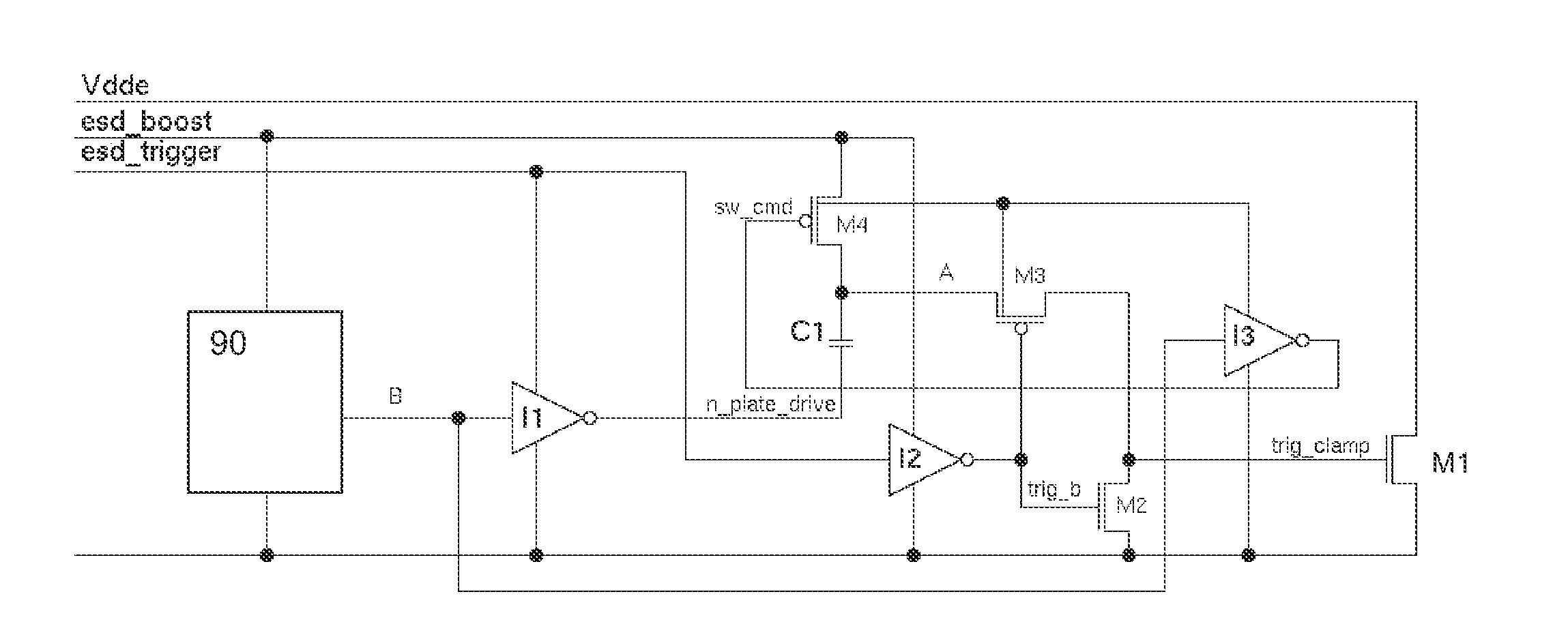
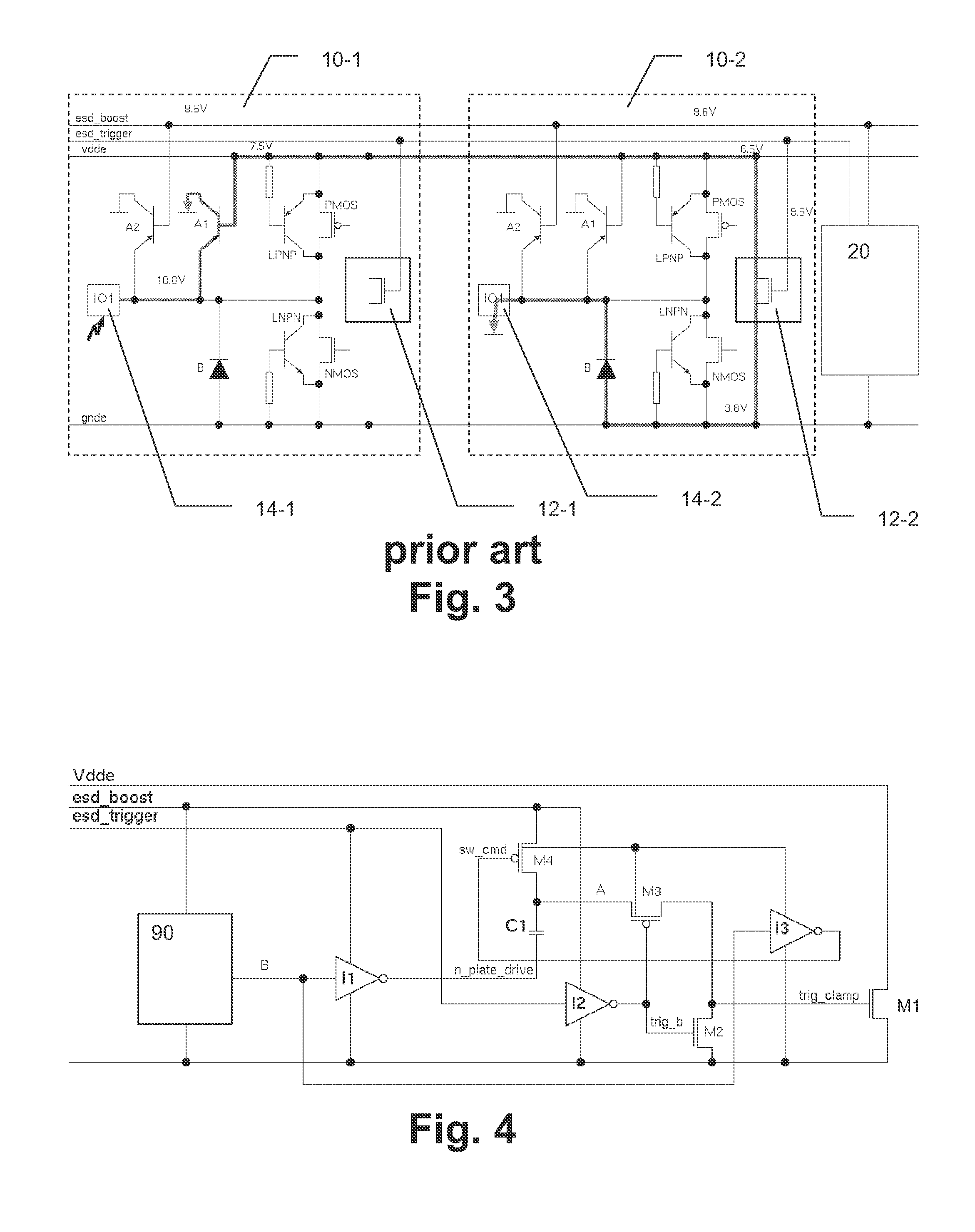
The present invention provides an improved method and protection circuit for protecting semiconductor circuits against temporary excessive voltage on a supply line. The protection circuit includes a clamp element that generates a low resistive path between the supply line and a lower reference potential, when activated. A trigger circuit generates a first trigger signal in response to detection of an excessive voltage on the supply line. An overdrive circuit activates the clamp element by applying a boosted second trigger signal at a voltage higher than the first trigger signal to a control terminal of the clamp element in response to the first trigger signal. This results in a reduced width of the clamp element, which leads to lower current leakage and faster and smaller transistors. The protection circuit can be integrated into the semiconductor circuit without modifying the I / O cell architecture. Additionally, the overdrive circuit may include an energy storing element selectively chargeable to a boosted voltage derived from the temporary excessive voltage, and a pulse forming circuit for initiating charging of the energy storing element prior to generation of the first trigger signal. The proposed protection circuit relies on the energy of the excessive voltage, which means that power supply is only needed during the excessive voltage event, while no clock signal or the like is required to rise the control voltage of the clamp element.

Problems solved by technology

This reduced width results in a lower current leakage.

Method used


Image

  • Protection circuit with overdrive technique
  • Protection circuit with overdrive technique
  • Protection circuit with overdrive technique

Examples


Embodiment Construction

[0025]The embodiments of the present invention will now be described in greater detail based on a ESD protection circuit for rail-based distributed ESD networks.

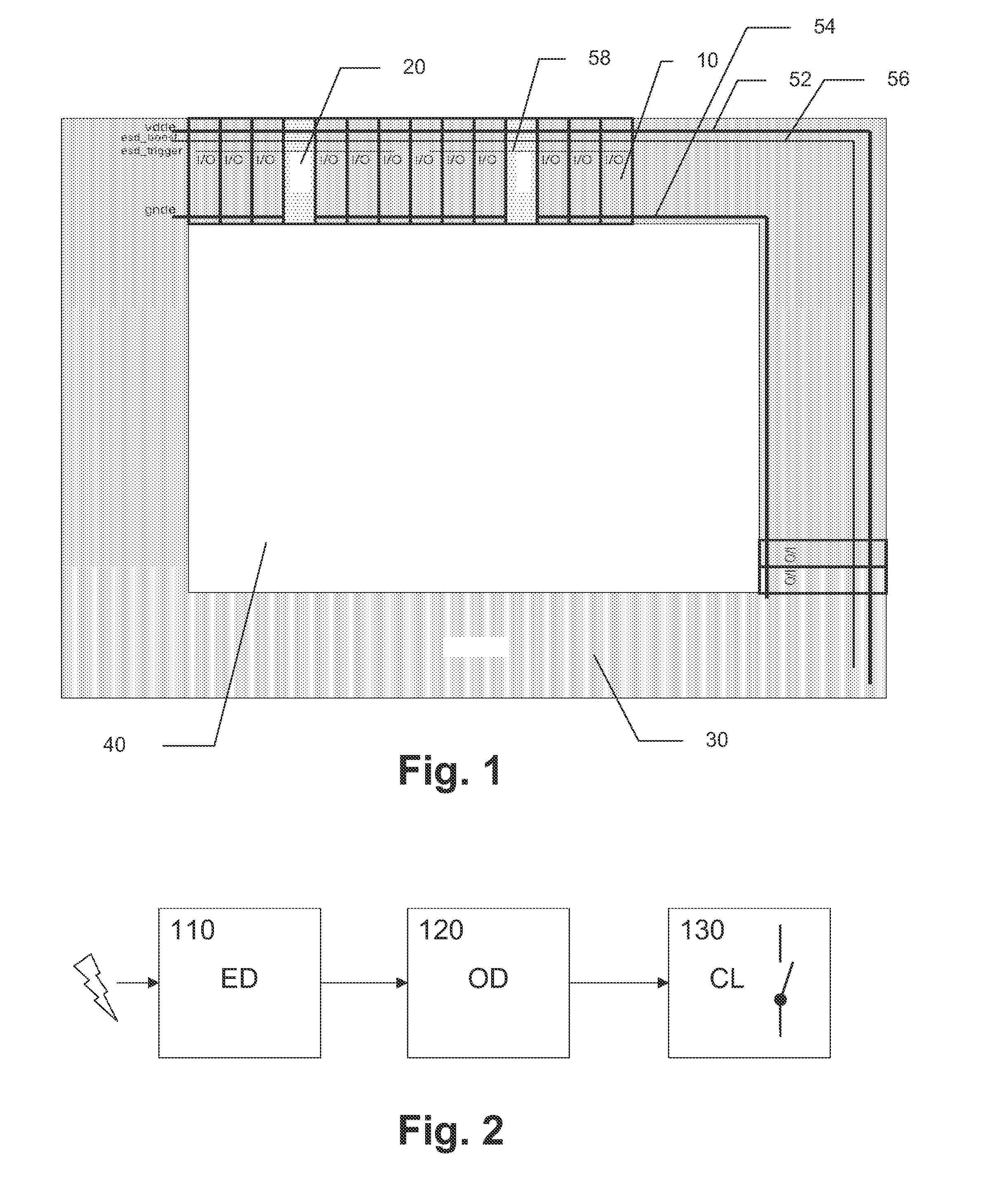
[0026]FIG. 1 shows an example of an integrated circuit according to the embodiment with I / O ring 30 and protection rails esd_boost 56 and esd_trigger 58 as described initially. Between the IC core 40 and the outside world, I / O cells 10 are organized in a ring to form the I / O ring 30. The I / O cells 10 are responsible for supply voltage level shifting for noise immunity and at the same time for excessive-voltage protection of the IC core 40, and receive their supply voltage from a supply rail vdde 52 and a ground rail gnde 54. Distributed trigger circuits 20 for triggering ESD clamps of the I / O cells 10 are placed between some of the I / O cells 10.

[0027]It is known that for an MOS transistor the drain current is proportional to W / L (VGS−VT)2, wherein W and L denote the gate width and length, respectively, VT denotes the thresho...


PUM


Abstract

The present invention relates to a protection circuit and method of protecting a semiconductor circuit against a temporary excessive voltage on a supply line, wherein a first trigger signal is generated in response to a detection of an excessive voltage on the supply line and a clamp element (M1) is activated by applying a boosted second trigger signal at a voltage higher than the first trigger signal to a control terminal of the clamp element (M1) in response to said first trigger signal, to thereby generate a low resistive path between said supply line and a lower reference potential. Thereby, the clamp element (M1) is activated with a higher voltage and can thus be made smaller in width. Because the clamp element is smaller, a remote trigger circuit can be sized tighter and faster.

Description

FIELD OF THE INVENTION[0001]The present invention relates to a protection circuit and method for protecting a semiconductor circuit against a temporary excessive voltage on a supply line The excessive voltage may be caused as a result of an electrostatic discharge (ESD) or other external noise or interference.BACKGROUND OF THE INVENTION[0002]In advanced complementary metal oxide semiconductor (CMOS) technologies gate oxides are very thin and operating on supply voltages (Vdd) are confined in small ranges, such as 1V for example. MOS transistor structures in the integrated circuit (IC) core are thus very fragile and high voltages can be generated by electrostatic charging in the manufacturing chain, at the chip assembly or in applications, which might destroy the IC.[0003]Between the IC core and the outside world, input / output (IO) cells may be organized in a ring, which are responsible for Vdd level shifting, for noise immunity, and—at the same time—for protection of the IC core fro...

Claims


Application Information

Patent Timeline
Patent Type & Authority Patents(United States)
IPC IPC(8): H02H3/22
CPCH01L27/0285
Inventor NEGOI, ANDY C.
Owner NXP BV
Learn More