
Image sensor including a pixel cell having an epitaxial layer, system having the same, and method of forming a pixel cell

a technology of image sensor and epitaxial layer, which is applied in the field of image sensors, can solve the problem of limiting the degree to which the effective depth of the photo diode region can be increased, and achieve the effect of reducing crosstalk between photo-converting devices and high quantization efficiency

Inactive Publication Date: 2012-04-24
SAMSUNG ELECTRONICS CO LTD
View PDF6 Cites 0 Cited by
  • Summary
  • Abstract
  • Description
  • Claims
  • Application Information

AI Technical Summary

Benefits of technology

The solution enables a deeper effective depth of the photo diode region without blooming, resulting in high quantization efficiency and reduced crosstalk between pixel cells, even when using the same ion implantation energy as conventional methods.

Problems solved by technology

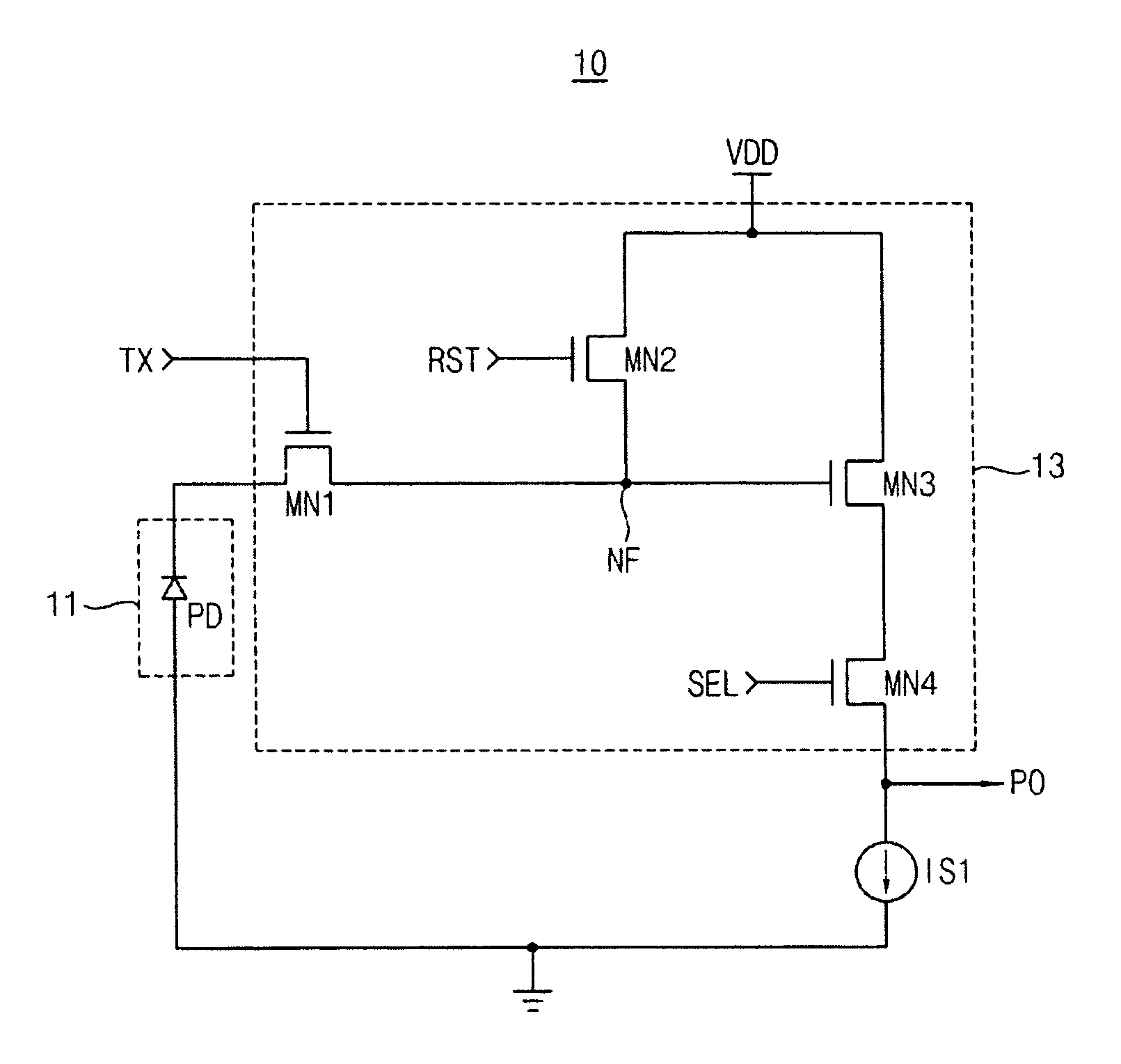
However, in the pixel cell of an image sensor having a stepped epitaxial layer or a graded epitaxial layer, there is a limit to the degree to which an effective depth of the photo diode region can be increased by raising energy of an ion beam in the ion implantation process.

Method used


Image

  • Image sensor including a pixel cell having an epitaxial layer, system having the same, and method of forming a pixel cell
  • Image sensor including a pixel cell having an epitaxial layer, system having the same, and method of forming a pixel cell
  • Image sensor including a pixel cell having an epitaxial layer, system having the same, and method of forming a pixel cell

Examples


Embodiment Construction

[0044]Detailed example embodiments are disclosed herein. However, specific structural and functional details disclosed herein are merely representative for purposes of describing example embodiments. Example embodiments may, however, be embodied in many alternate forms and should not be construed as limited to only the embodiments set forth herein.

[0045]Accordingly, while example embodiments are capable of various modifications and alternative forms, embodiments thereof are shown by way of example in the drawings and will herein be described in detail. It should be understood, however, that there is no intent to limit example embodiments to the particular forms disclosed, but to the contrary, example embodiments are to cover all modifications, equivalents, and alternatives falling within the scope of example embodiments. Like numbers refer to like elements throughout the description of the figures.

[0046]It will be understood that, although the terms first, second, etc. may be used h...


PUM


Abstract

A pixel cell includes a substrate, an epitaxial layer, and a photo converting device in the epitaxial layer. The epitaxial layer has a doping concentration profile of embossing shape, and includes a plurality of layers that are stacked on the substrate. The photo converting device does not include a neutral region that has a constant potential in the vertical direction. Therefore, the image sensor including the pixel cell has high quantization efficiency, and a crosstalk between photo-converting devices is decreased.

Description

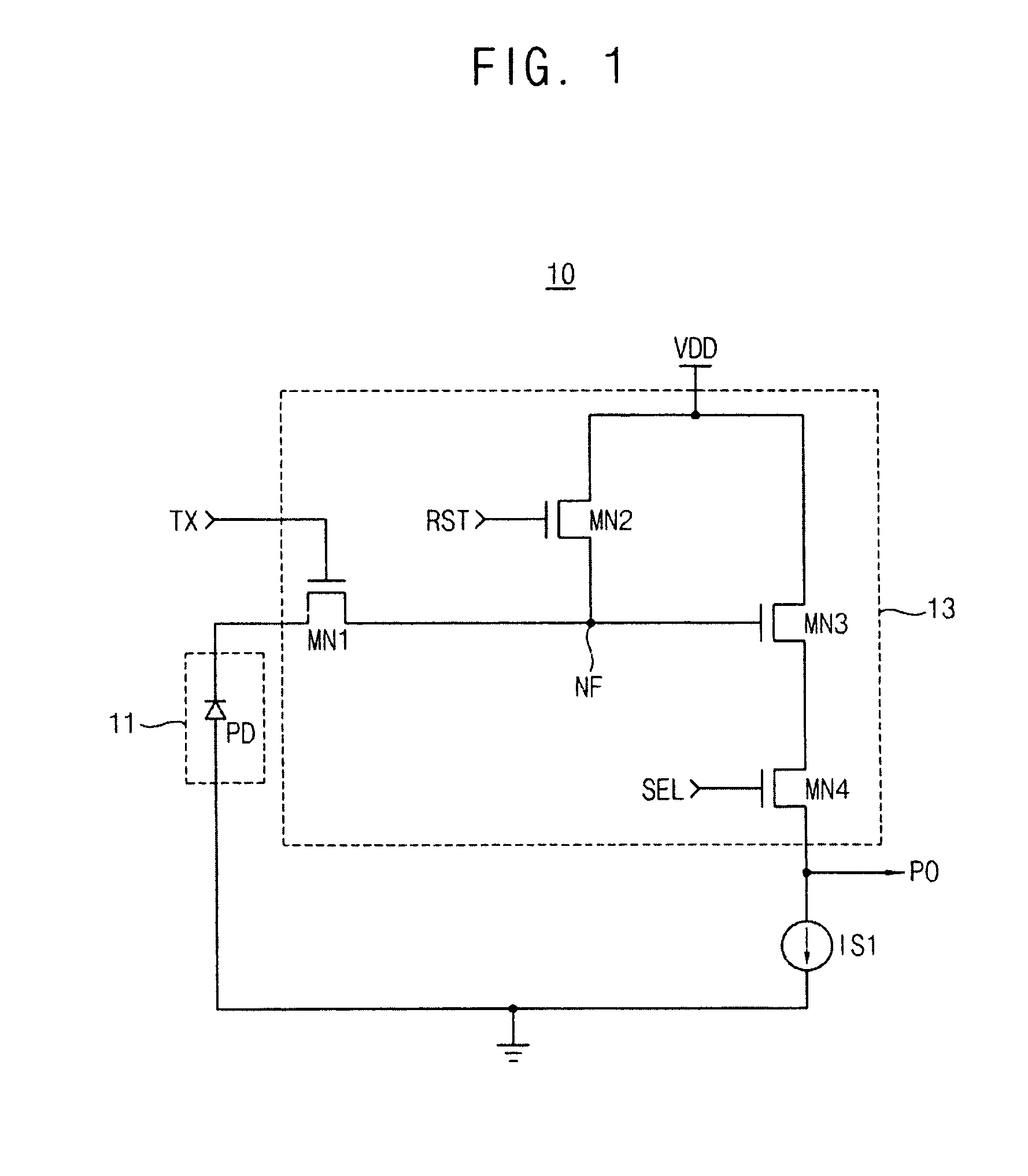
CROSS-REFERENCE TO RELATED APPLICATIONS[0001]This application claims priority under 35 USC §119 to Korean Patent Application No. 10-2008-0090981, filed on Sep. 17, 2008 in the Korean Intellectual Property Office (KIPO), the entire contents of which are incorporated herein by reference.BACKGROUND[0002]1. Technical Field[0003]The embodiments relate to an image sensor, and more particularly to a pixel cell having a plurality of epitaxial layers, a CMOS image sensor including the pixel cell, and a method of forming a pixel cell of the CMOS image sensor.[0004]2. Description of the Related Art[0005]A complementary metal oxide semiconductor (CMOS) image sensor is widely used as an image capturing device because it has low operating voltage, low power consumption, and low production cost. The CMOS image sensor includes a pixel cell array composed of a plurality of pixel cells. Each of the pixel cells may include a photo diode, a transfer transistor, a reset transistor, a source follower tra...

Claims


Application Information

Patent Timeline
Patent Type & Authority Patents(United States)
IPC IPC(8): H01L31/113H04N25/00
CPCH01L27/1463H01L27/14643H01L27/14689H01L27/146
Inventor LEE, KYUNG-HOJUNG, KWANG-ILAHN, JUNG-CHAKKIM, YI-TAEMOON, KYOUNG-SIKKIM, BUM-SUKKEE, YOUNG-BAELEE, DONG-YOUNGJUNG, TAE-SUBLEE, KANG-SUN
Owner SAMSUNG ELECTRONICS CO LTD
Learn More