Memory modules and methods for modifying memory subsystem performance

a memory subsystem and memory module technology, applied in the field of memory subsystems, can solve the problems of performance bottlenecks, difficult retroactively changing the power plane design of the motherboard, and compromising the reliability of the memory controller, so as to optimize the performance of the memory subsystem

Active Publication Date: 2012-04-24
KIOXIA CORP
View PDF10 Cites 0 Cited by
  • Summary
  • Abstract
  • Description
  • Claims
  • Application Information

AI Technical Summary

Benefits of technology

[0014]In view of the above, it can be seen that technical effects associated with the invention include the ability to achieve a higher memory core supply voltage (VDD) as compared to the I / O supply voltage (VDDQ) on a memory module, which allows for higher frequency and latency yield without compromising the memory controller that manages the flow of data to and from the module. The ability to selectively boost the core supply voltage without increasing bus voltage avoids voltage level mismatch between the memory I / O and chipset I / O buffers. The invention also offers the advantage of an uncomplicated implementation at the memory module PCB level without requiring any redesign of existing motherboards, and avoids additional costs on the motherboard for implementing a separate memory VDD voltage regulator module.

Problems solved by technology

System memory has become one of the performance bottlenecks in current computer configurations.
A drawback of increasing the DRAM supply voltage is that all current DRAM implementations in standard computer systems specify a single supply voltage plane for both the core voltage (VDD) and the input / output voltage (VI / O or VDDQ) on both the motherboard and memory circuit board level, even though the two power planes are separate on all current DRAM chip levels.
Increasing the I / O voltage, however, can compromise the reliability of the memory controller.
The sensitivity to overvoltage and the associated reliability problems become particularly important if the memory controller is integrated into the central processor unit (CPU), as in the current models offered by Advanced Micro Devices, Inc.
However, it is difficult to retroactively change designs of the power planes of motherboards in order to separate supply voltages for the DRAM core and I / O circuitry.
In this case it is also advantageous that the termination voltage on the motherboard remains unchanged at one-half of the original supply voltage, since it has been empirically found that increasing the termination voltage of the I / O system above the center of the voltage swing increases performance, whereas lowering the termination voltage below the midpoint of the voltage swing is generally detrimental to performance.
A potential drawback of the lowered memory VDDQ is that the memory voltage is supplied not only to the memory but also to the I / O portion of the memory controller.
One limitation to overcome in this situation is that most current memory designs utilize internal voltage regulators to keep the core voltage at a predefined level that is lower than the supply voltage.

Method used


Image

  • Memory modules and methods for modifying memory subsystem performance
  • Memory modules and methods for modifying memory subsystem performance
  • Memory modules and methods for modifying memory subsystem performance

Examples


Embodiment Construction

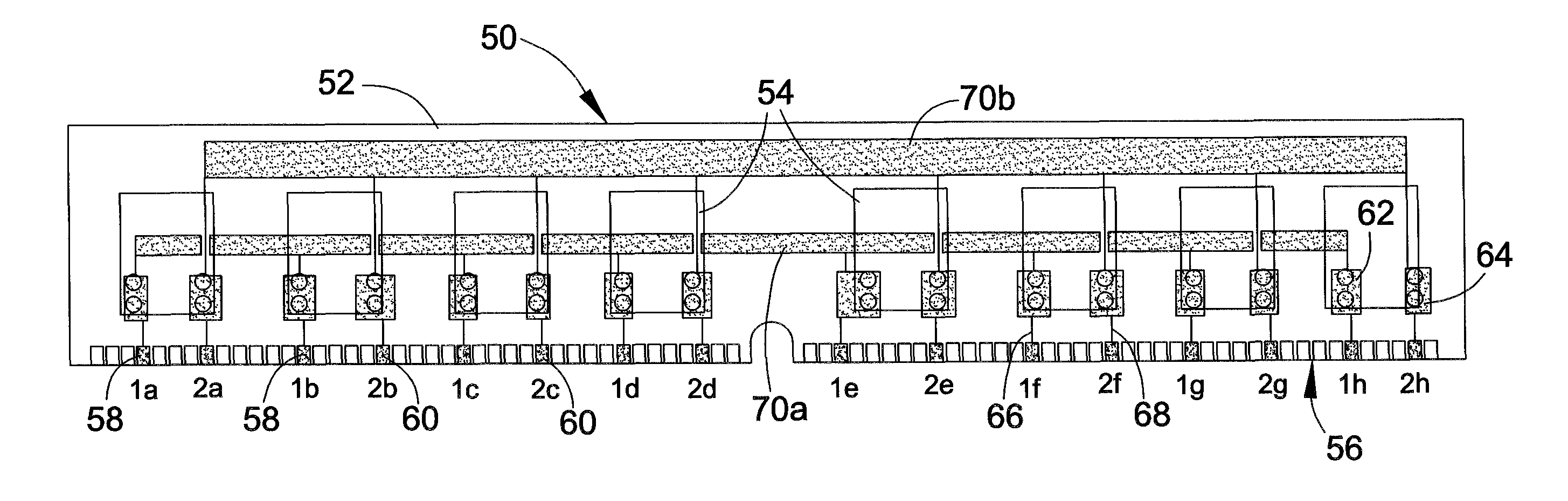
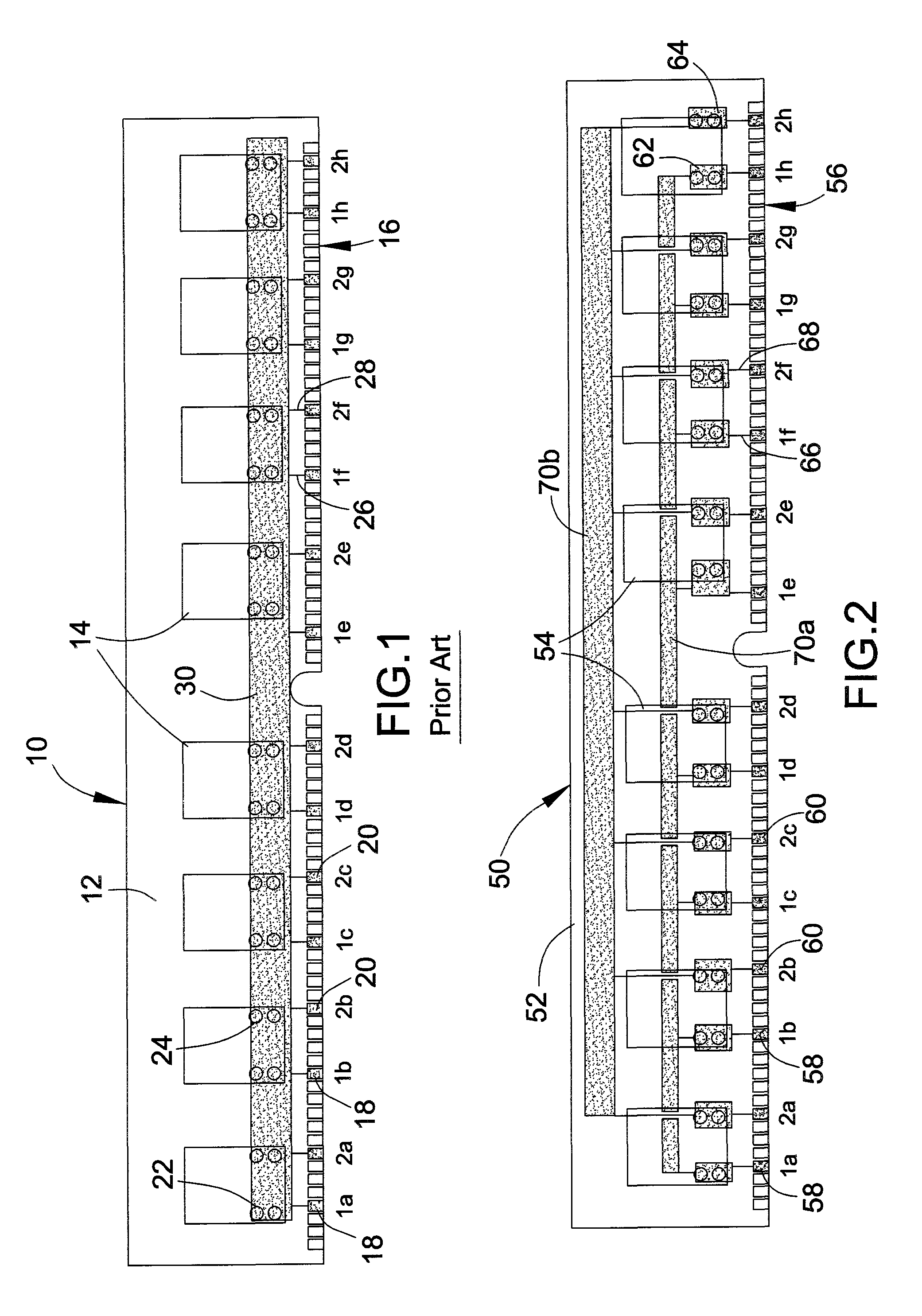
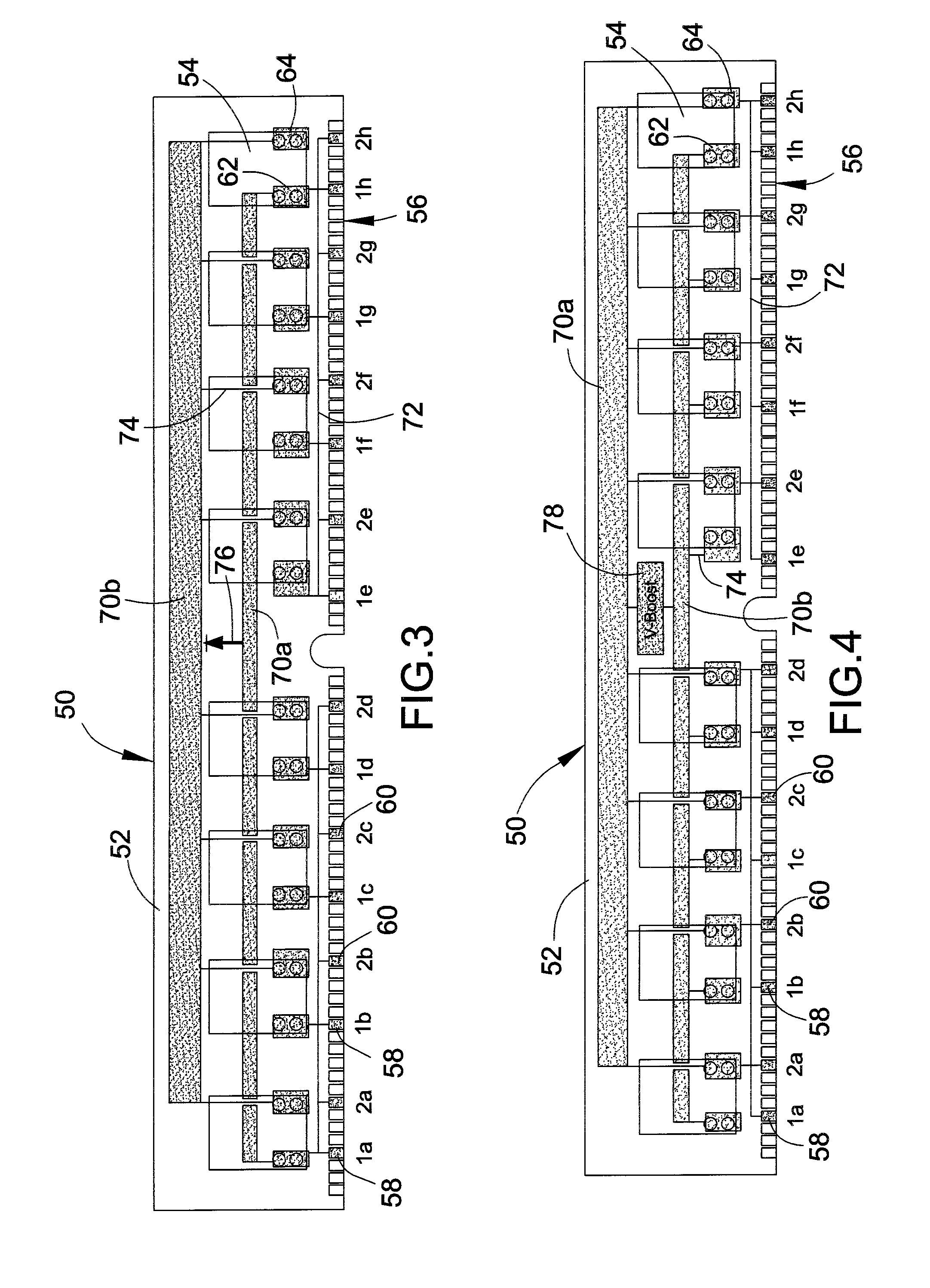
[0021]FIGS. 2 through 5 schematically represent memory modules 50 configured to allow different supply voltages to be supplied to the core (VDD) and I / O portions (VDDQ) of memory components (chips) 54 on the modules 50. For convenience, consistent reference numbers are used throughout FIGS. 2 through 5 to identify the same or functionally equivalent elements.

[0022]Similar to the memory module 10 of FIG. 1, the memory chips 54 of each memory module 10 schematically represented in FIGS. 2 through 5 are mounted on a PCB 52 having an edge connector 56 comprising individual pins, some of which are VDD (core supply) input pins 58 and others are VDDQ (I / O) input pins 60. In contrast to the module 10 of FIG. 1, VDD and VDDQ input pins 62 and 64 of the chips 54 are not at the same voltage as a result of being connected to the pins 58 and 60 through a common voltage plane, but instead receive their voltage from primary and secondary voltage planes 70a and 70b on the PCB 52. The voltage planes...


PUM


Abstract

Methods and memory modules adapted for use in computer systems to generate different voltages for core supply (VDD) and input / output supply (VDDQ) inputs to memory components of the computer memory subsystem. The memory module includes a substrate with an edge connector, a memory component, and first and second voltage planes adapted to supply the core supply voltage and the input / output supply voltage to the memory component. The first voltage plane receives a system input voltage from the edge connector, and the second voltage plane is connected to the first voltage plane to receive a second voltage that is either higher or lower than the system input voltage. One of the first and second voltage planes is connected to the memory component to supply the core supply voltage thereto, and the other voltage plane supplies the input / output supply voltage to the memory component.

Description

CROSS REFERENCE TO RELATED APPLICATIONS[0001]This application claims the benefit of U.S. Provisional Application No. 61 / 120,119, filed Dec. 5, 2008, the contents of which are incorporated herein by reference.BACKGROUND OF THE INVENTION[0002]The present invention generally relates to memory subsystems and related components of computer systems. More particularly, this invention relates to methods and circuitry for altering and preferably optimizing the performance of a memory subsystem by generating different voltages for VDD and VDDQ inputs to memory components of the memory subsystem.[0003]System memory has become one of the performance bottlenecks in current computer configurations. Memory signaling frequencies are doubling roughly every five years in order to keep up with the increased bandwidth requirements of modern system architectures. At the same time, the supply voltage of the memory subsystem is lowered in the process of transitioning to smaller process nodes. However, a r...

Claims


Application Information

Patent Timeline
Patent Type & Authority Patents(United States)
IPC IPC(8): G11C5/02G11C17/18
CPCG11C5/04G11C5/063G11C5/14H05K1/0262H05K1/117H05K2201/093H05K2201/09663H05K2201/10159
Inventor SCHUETTE, FRANZ MICHAELALLEN, WILLIAM J.
Owner KIOXIA CORP
Why Eureka
Try Eureka