
Semiconductor chip pad structure and method for manufacturing the same

a semiconductor and chip pad technology, applied in semiconductor devices, semiconductor/solid-state device details, electrical apparatus, etc., can solve the problems of affecting the electric reliability, and affecting the yield rate of led packaging elements

Inactive Publication Date: 2012-05-01
ARIMA OPTOELECTRONICS
View PDF11 Cites 0 Cited by
  • Summary
  • Abstract
  • Description
  • Claims
  • Application Information

AI Technical Summary

Benefits of technology

"The invention provides a semiconductor chip pad structure and a method for manufacturing it that ensures the quality of the ball bond. The structure includes a flat area at the center and a roughened area at the periphery. The flat area provides adhering force for the ball bond while the roughened area prevents vibrating energy from affecting the terminal pad. The proportion of the central flat area to the total surface area of the terminal pad is 50 to 90%. The method includes steps of defining the central area of the terminal pad, roughening the surface layer of the semiconductor chip outside the mask, and evaporating the metal material of the terminal pad onto the flat and roughened areas of the surface layer of the semiconductor chip. The terminal pad has a flat area at the center and a roughened area at the periphery. The surface layer of the semiconductor chip is constructed as LED light-emitting layer. The technical effect of the invention is to improve the reliability and stability of the semiconductor chip pad structure."

Problems solved by technology

Any mechanic devices have their own mechanic difference and fluctuation that tend to cause an undesired wire-bonding shift for the ball bond.
Accordingly, the pressure and the ultrasonic energy will be abnormally and asymmetrically delivered to the area of the light-emitting layer adjacent to the pad.
In this way, it is likely to do direct harm to the light-emitting layer when the light-emitting layer (made of AlInGaP) of LED is not hard enough or when it is roughened by a special treatment.
Damages like cracks or the cratering may take place and cause an adverse effect on the yield rate of the LED packaging elements as well as on the electric reliability.

Method used


Image

  • Semiconductor chip pad structure and method for manufacturing the same
  • Semiconductor chip pad structure and method for manufacturing the same
  • Semiconductor chip pad structure and method for manufacturing the same

Examples


Embodiment Construction

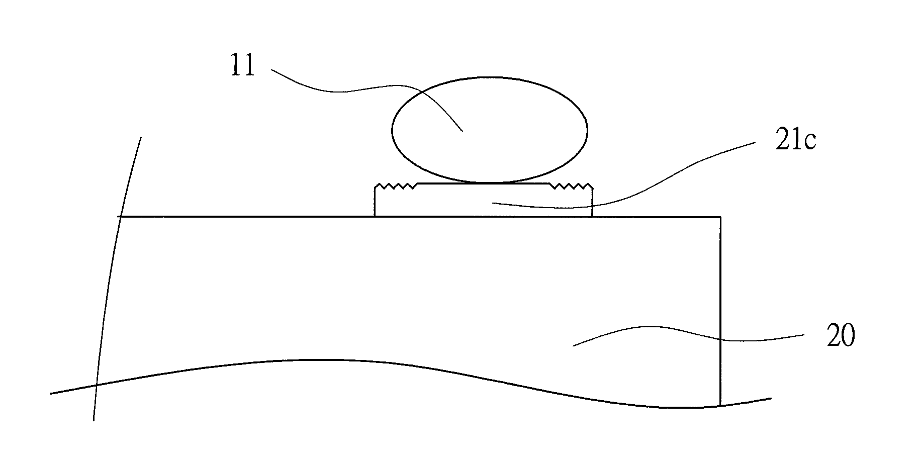
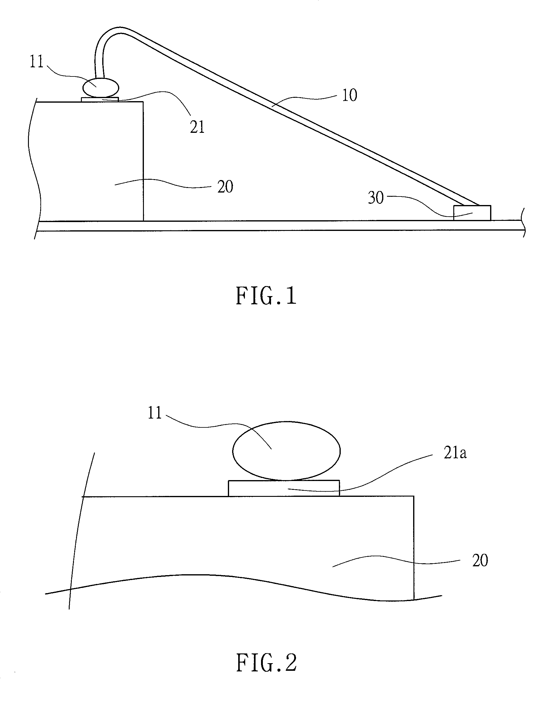
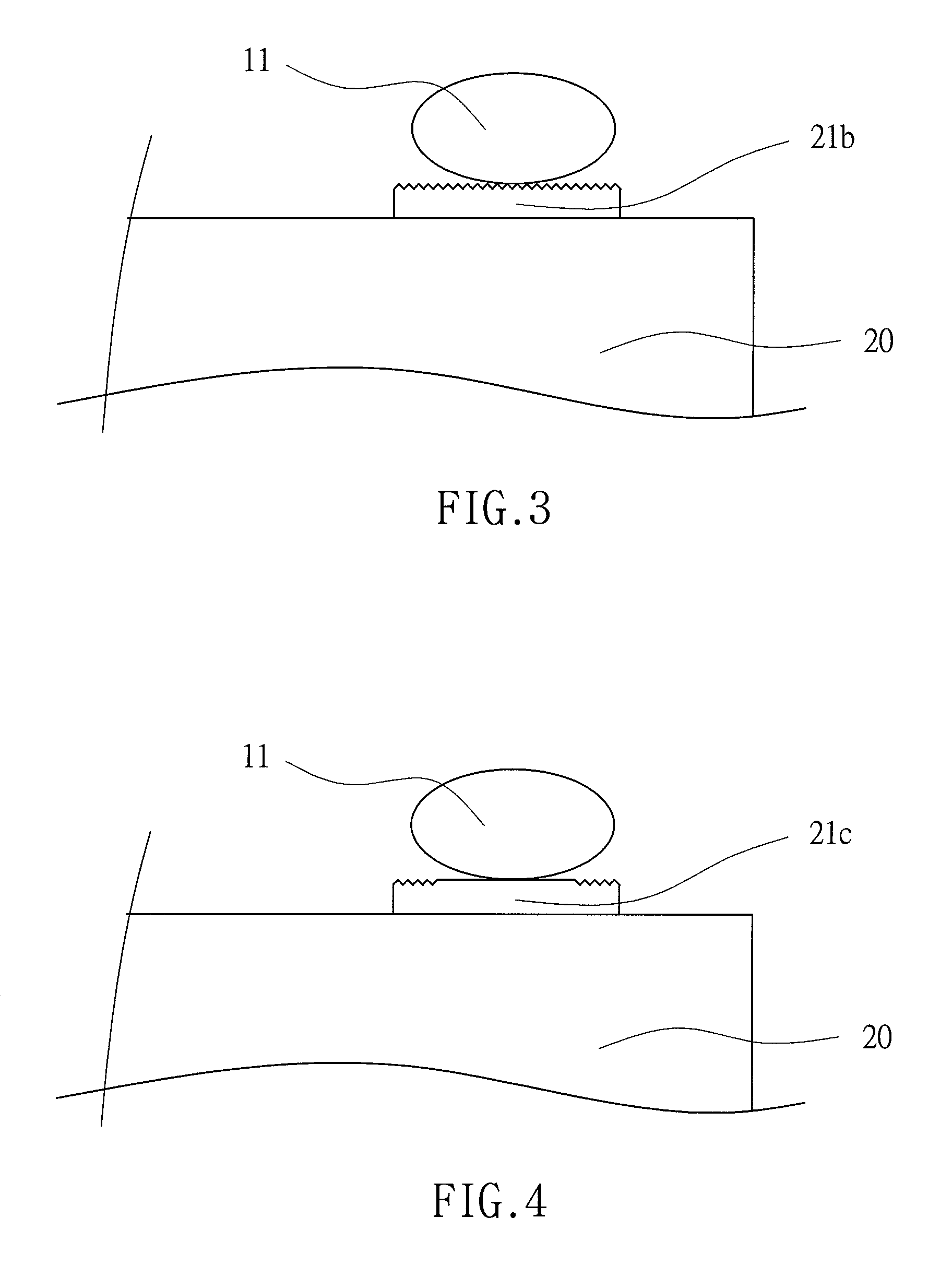
[0025]First of all, referring to FIG. 2, the surface of the terminal pad 21a of a conventional semiconductor chip 20 is designed to be a flat surface. As shown in FIG. 3, a terminal pad 21b having a roughened surface is positioned on the same surface layer (such as LED light-emitting layer) of the semiconductor chip 20. The results of the wire-bonding process applied to the ball bond 11 of the two above-mentioned arrangements indicate that the terminal pad 21b having the roughened surface may resist more against the ultrasonic vibration than the terminal pad 21a having the flat surface. The reason lies in that the transverse transmission of energy tends to be hindered by the roughened surface. In other words, it is difficult to transmit the vibrating energy of the ultrasonic wave from both sides of the terminal pad 21b having the roughened surface to the bottom. Therefore, it is more unlikely to cause crack or cratering of the chip (with the terminal pad 21b having the roughened sur...


PUM


Abstract

A semiconductor chip pad structure and a method for manufacturing the same, wherein a flat area at the center of the terminal pad and a roughened area at the periphery thereof are provided by use of the mask photolithograph technique and the roughening process. The central area provides a sufficient adhering force for the ball bond while the peripheral area prevents the wire-bonding vibrating energy from the lateral transmission to the external side of the terminal pad. In this way, the ball bond for the terminal pad may meet the wire-bonding requirements. Moreover, the ball bond quality is ensured.

Description

BACKGROUND OF THE INVENTION[0001]1. Field of the Invention[0002]The invention relates to a semiconductor chip pad structure and a method for manufacturing the same, and more particularly to an arrangement with a flat area at the center of the terminal pad and a roughened area at the periphery thereof.[0003]2. Description of the Related Art[0004]Light-emitting diodes (LED) have a small size and a high luminous efficiency. Moreover, they are able to emit a light having different colors, thereby ensuring a various application. As a result, a lot of packaging (assembly) shapes have been created. The packaged products are generally known as lamps or SMD (surface mounting device). Apart from the appearance, another important consideration point is the quality reliability. Therefore, the wire bonding is an important step for both the lamp arrangement and the SMD-arrangement before or after the packaging process. The wire bonding is done for fitting a metal pad to the positive side of the L...

Claims


Application Information

Patent Timeline
Patent Type & Authority Patents(United States)
IPC IPC(8): H01L23/48H01L23/52
CPCH01L24/03H01L24/05H01L24/48H01L33/38H01L2924/12041H01L2924/01033H01L2924/01006H01L2224/451H01L33/62H01L2224/04042H01L2224/05556H01L2224/05557H01L2224/05599H01L2224/4807H01L2224/48091H01L2224/48227H01L2224/4845H01L2224/48465H01L2224/85399H01L2924/01005H01L2924/01082H01L2924/00014H01L2224/45099H01L2924/00H01L24/45H01L2924/00015
Inventor WANG, HUI-HENG
Owner ARIMA OPTOELECTRONICS
Learn More