Defective pixel detecting device, defective pixel detecting method, record medium storing a program for detecting defective pixels, and imaging apparatus

a technology for defective pixels and solid-state imaging devices, which is applied in the direction of color television details, television systems, television systems, etc., can solve the problems of limited amount of defection data that can be stored, image degradation due to imaging output of such defective pixels, and defected pixels in solid-state imaging devices such as ccds made of semiconductors, etc., to reduce adverse effects of temperature differences, reduce image degradation, and reduce the effect of image degradation

Active Publication Date: 2012-05-01
PANASONIC CORP
View PDF6 Cites 23 Cited by
  • Summary
  • Abstract
  • Description
  • Claims
  • Application Information

AI Technical Summary

Benefits of technology

[0019]According to the above aspects, it is possible to diminish image degradation even if pixels that are actually defective and to be corrected are not detected in immediate defective pixel detection. Specifically, pixels that are stored in a defect information storing memory as defective pixels in a previous defection detecting process are highly possibly stored as defective pixels again in a defective pixel detecting process of this time, thereby diminishing the image degradation. Further, the priority is assigned to the defects in the same defective pixel detection result, and the correction targets are newly determined based on comparison with the priority of the past correction targets, and therefore it is possible to reduce adverse effects of differences in temperature and charge accumulation time that can occur due to differences in timing of the defective pixel detection, thereby allowing adequate detection of the pixels to be corrected.

Problems solved by technology

Solid-state imaging devices such as CCDs made of semiconductor often include defective pixels due to local crystal defects in the semiconductor.
It is known that image degradation due to imaging output of such defective pixels, or so-called white spots or black spots, may occur in an image taken by a solid-state imaging device including the defective pixels.
When actually mounting such a defect detecting and correcting system in a device such as a video camera, an amount of defection data that can be stored is limited by a storage capacity of a memory mounted in the device.
Therefore, when a number of the defective pixels that are present is over the storage capacity of the memory, defection data for defective pixels that are detected after the number of detected defective pixels exceeds the memory capacity cannot be stored in the memory.
Thus, a problem has been noted that defects are corrected only for a first half of the screen, for example.
However, according to the above described conventional configurations, it is possible to carry out defective pixel correction by selecting a pixel with higher priority from the pixels that have been detected during the defective pixel detection, but there is a problem that no countermeasure is taken in a case when a pixel that should be normally corrected cannot be detected.
Further, defective pixel has a property of changing the signal level according to temperature and charge accumulation time.
If the defection level of a defective pixel is accidentally low during the defective pixel detection, such a defective pixel cannot be detected, and accordingly possibly remains uncorrected.
Specifically, pixels that are stored in a defect information storing memory as defective pixels in a previous defection detecting process are highly possibly stored as defective pixels again in a defective pixel detecting process of this time, thereby diminishing the image degradation.

Method used


Image

  • Defective pixel detecting device, defective pixel detecting method, record medium storing a program for detecting defective pixels, and imaging apparatus
  • Defective pixel detecting device, defective pixel detecting method, record medium storing a program for detecting defective pixels, and imaging apparatus
  • Defective pixel detecting device, defective pixel detecting method, record medium storing a program for detecting defective pixels, and imaging apparatus

Examples


first embodiment

(First Embodiment)

1. Configuration

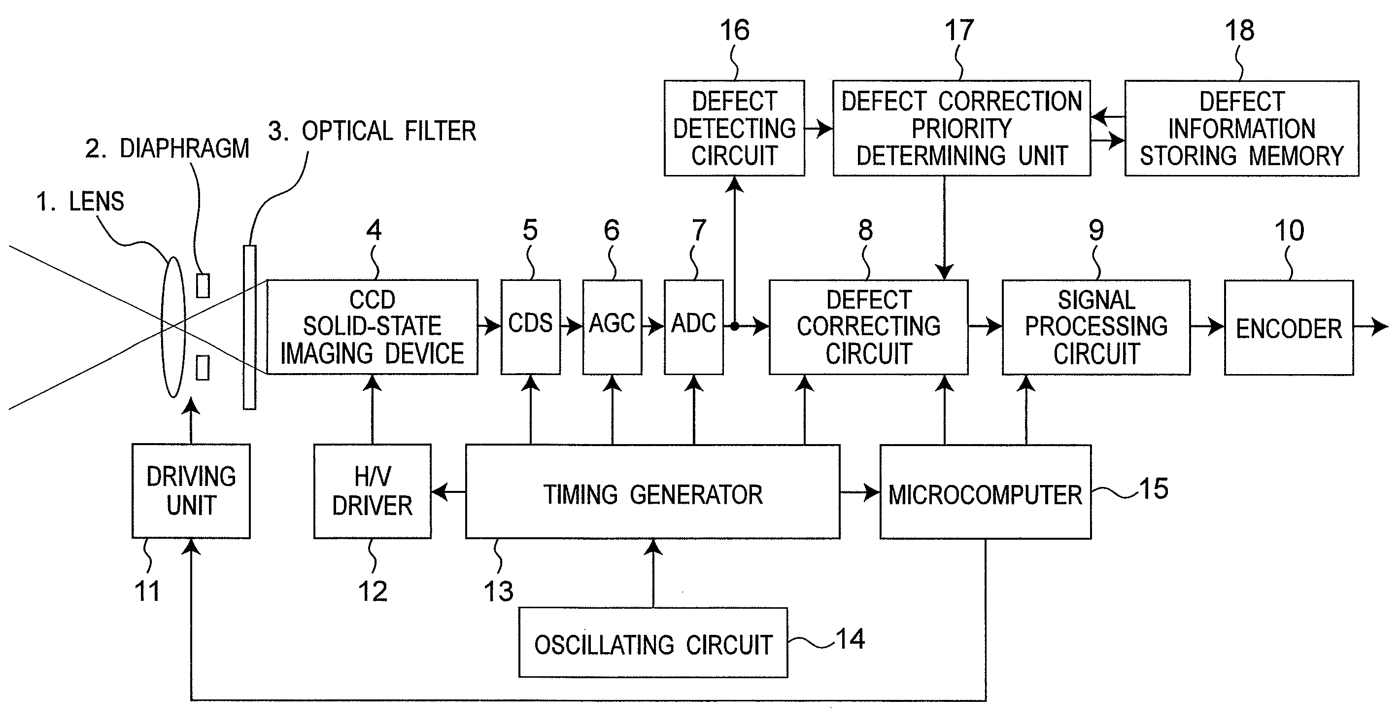
[0031]FIG. 1 is a block diagram illustrating a configuration of a video camera to which a defective pixel correcting apparatus according to a first embodiment is applied. This embodiment explains an example in which defect (white spot) correction is carried out by applying the defective pixel correcting apparatus to a video camera using a CCD solid-state imaging device.

[0032]The video camera is provided with a lens 1, a diaphragm 2, an optical filter 3, a CCD solid-state imaging device 4, a CDS (correlated double sampling circuit) 5, an AGC (automatic gain control circuit) 6, an ADC (A / D converter) 7, a defect correcting circuit 8, a signal processing circuit 9, an encoder 10, a driving unit 11, an H / V driver 12, a timing generator 13, an oscillating circuit 14, and a microcomputer 15.

[0033]An image of a subject is formed on an imaging plane of the CCD solid-state imaging device 4 via an optical system including the lens 1, the diaphragm 2, and the ...

second embodiment

(Second Embodiment)

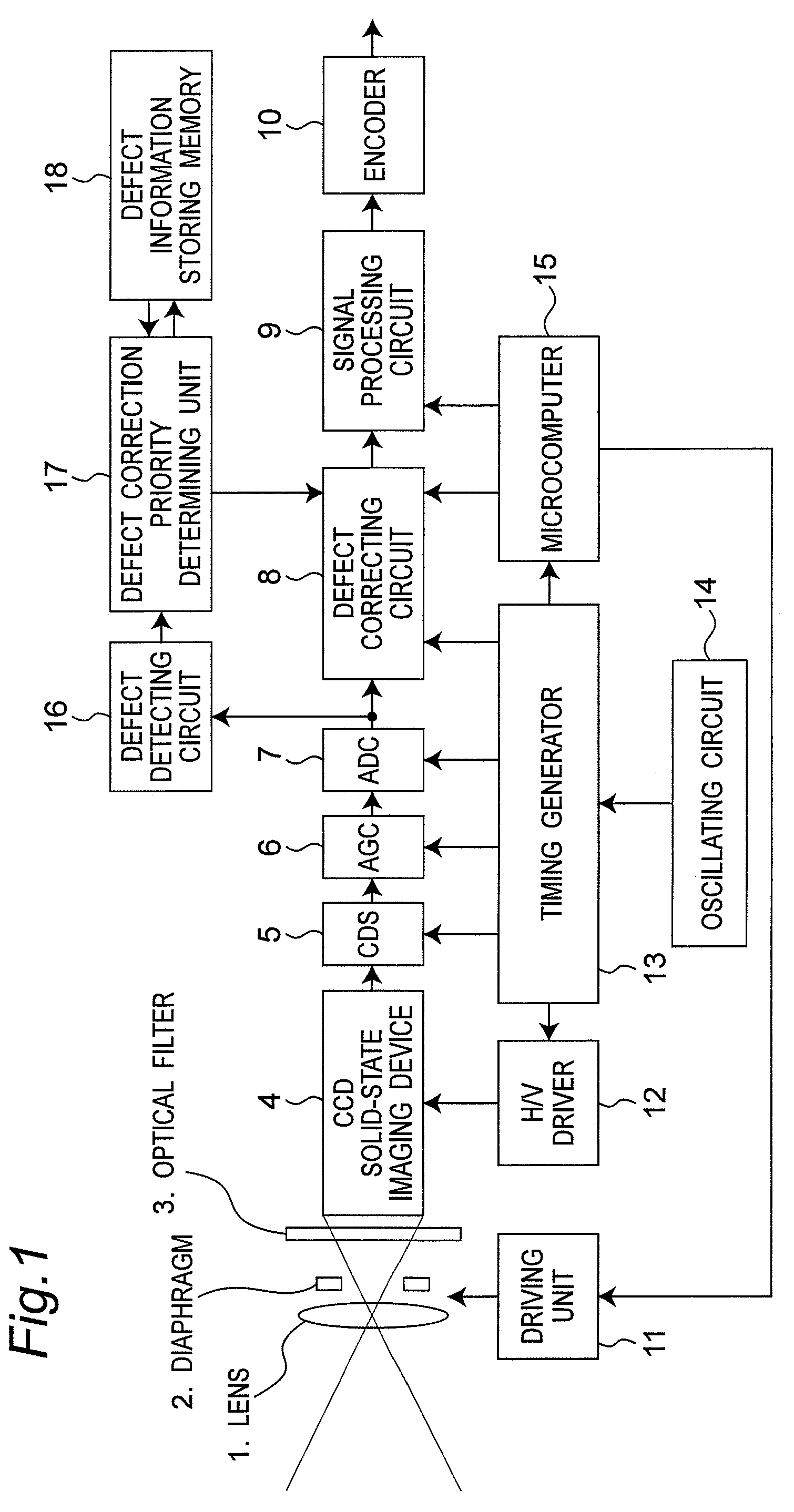
[0062]FIG. 5 is a block diagram illustrating a configuration of a video camera to which a defective pixel correcting apparatus according to a second embodiment is applied. This embodiment also explains an example in which defect (white spot) correction is carried out by applying the defective pixel correcting apparatus to a video camera using a CCD solid-state imaging device.

[0063]This embodiment is different from the first embodiment in that the function of the defect correction priority determining unit 17 according to the first embodiment is realized by the microcomputer 15, and the other configuration is basically the same.

[0064]In the defect information storing memory 18, the position information and the defect correction priority of the defective pixels that have been selected as the correction target pixels in the immediately previous defective pixel detecting process are stored. The rank order of priority of correction of the defective pixels is determined...


PUM


Abstract

A defective pixel detecting device determining defective pixels as correction targets in an imaging device that produces image signals is provided, and the device includes: defect information storage configured to store priority of defective pixels to be corrected; a defective pixel detector configured to detect defective pixels by comparing levels of imaging signals from the imaging device with a predetermined detection level; a priority setter configured to set priority of the detected defective pixels, based on the levels of the imaging signals of the defective pixels detected by the defective pixel detector; and a correction target determiner configured to newly determine defective pixels to be corrected based on the priority of the defective pixels out of the defective pixels that are currently detected by the defective pixel detector and the defective pixels to be corrected stored in the defect information storage, determining priority of the newly determined defective pixels to be corrected, and storing the priority of the newly determined defective pixels to be corrected in the defect information storage.

Description

BACKGROUND ART[0001]1. Technical Field[0002]The technical field relates to a defective pixel detecting device for detecting defective pixels of a solid-state imaging device, a defective pixel detecting method, a recording medium storing a program for detecting defective pixels, and an imaging apparatus.[0003]2. Related Art[0004]Solid-state imaging devices such as CCDs made of semiconductor often include defective pixels due to local crystal defects in the semiconductor. It is known that image degradation due to imaging output of such defective pixels, or so-called white spots or black spots, may occur in an image taken by a solid-state imaging device including the defective pixels.[0005]Accordingly, in the recent years, a defect detecting and correcting system has been proposed that detects and corrects defective pixels with a solid-state imaging device being set in a video camera and such. With this type of defect detecting and correcting systems, when scanning and detecting within...

Claims


Application Information

Patent Timeline
Patent Type & Authority Patents(United States)
IPC IPC(8): H04N9/64H04N5/335H04N5/367H04N5/372
CPCH04N5/367H04N25/68
Inventor WATANABE, SETSUKOIWAI, NOBUO
Owner PANASONIC CORP
Why Eureka
Try Eureka