Method of fabricating a conductive post on an electrode

a technology of conductive posts and electrodes, applied in the field of semiconductor devices, can solve the problems of forming cracks in dielectric films on electrode pads, creating residues (e.g., debris from electrode pads) remaining on electrode pads, etc., and achieve good electric characteristics of fabricated semiconductor devices. , the effect of preventing the formation of cracks

Active Publication Date: 2012-05-22
LAPIS SEMICON CO LTD
View PDF7 Cites 5 Cited by
  • Summary
  • Abstract
  • Description
  • Claims
  • Application Information

AI Technical Summary

Benefits of technology

[0009]According to the above aspects of the present invention, it is possible to prevent cracks in dielectric films formed on the electrode pads even if the wafer inspection using a probe machine is employed, resulting in good electric characteristics of the fabricated semiconductor device.

Problems solved by technology

The wafer inspection, however, may create residues (e.g., debris from the electrode pads) remaining on the electrode pads by bringing the probe needles in contact with the electrode pads.
The residues may lead to cracks in dielectric films formed on the electrode pads in the pad redistribution step.
The cracks may cause any damage such as short-circuiting to semiconductor chips.

Method used


Image

  • Method of fabricating a conductive post on an electrode
  • Method of fabricating a conductive post on an electrode
  • Method of fabricating a conductive post on an electrode

Examples


Embodiment Construction

[0018]Further scope of applicability of the present invention will become apparent from the detailed description given hereinafter. However, it should be understood that the detailed description and specific examples, while indicating preferred embodiments of the invention, are given by way of illustration only, since various changes and modifications will become apparent to those skilled in the art from the detailed description.

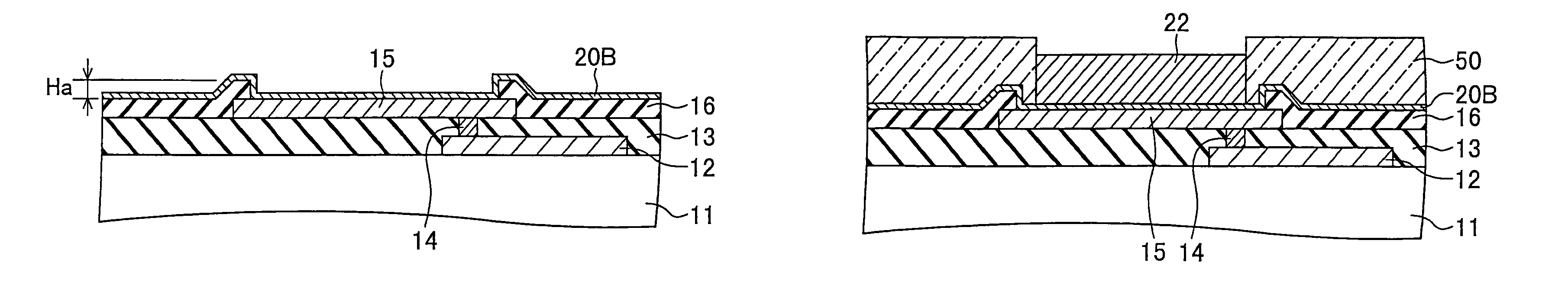
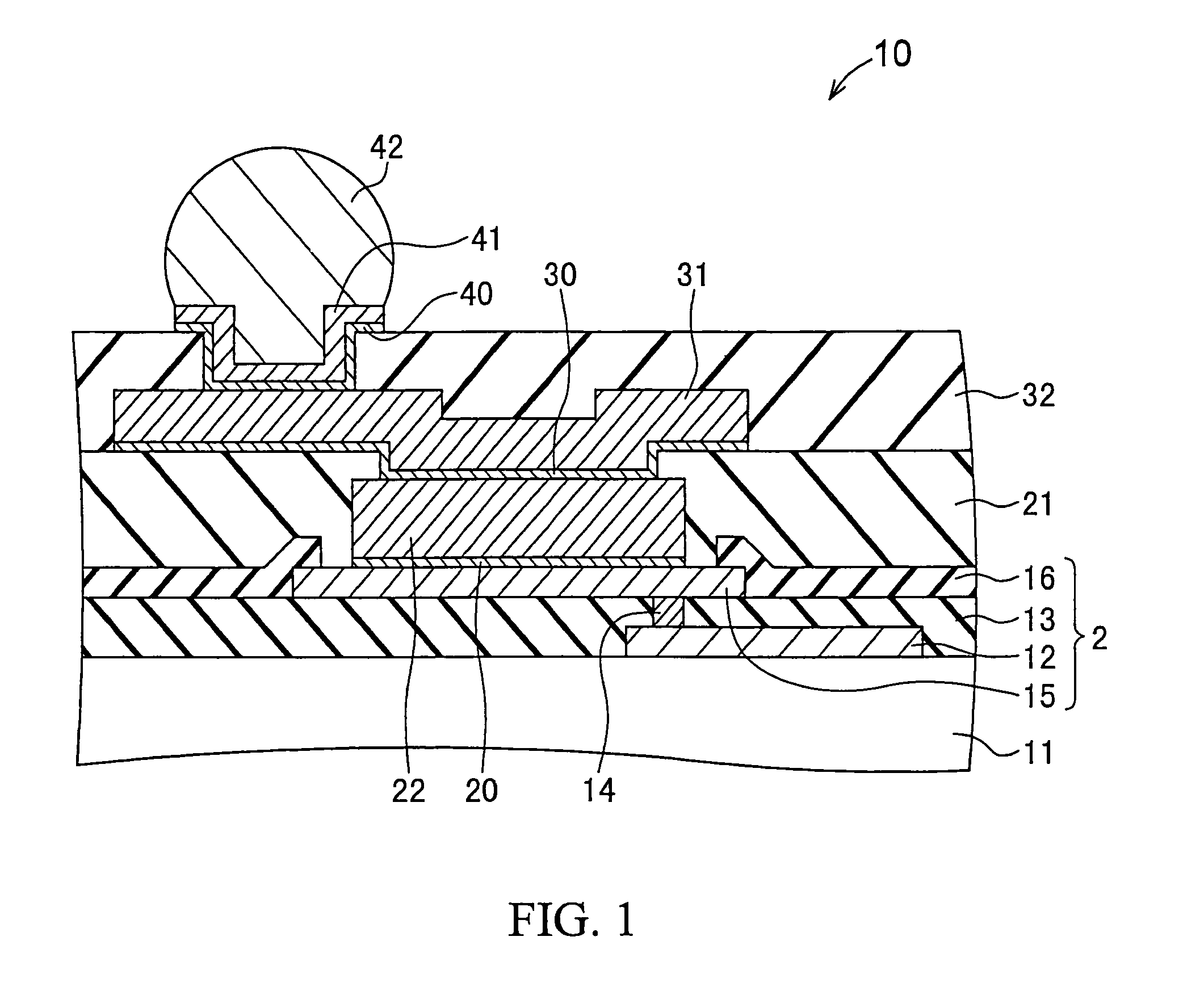
[0019]FIG. 1 is a cross-sectional view schematically illustrating an example of a semiconductor device 10 according to an embodiment of the present invention. As illustrated in FIG. 1, the semiconductor device 10 includes a semiconductor substrate 11 and an upper structure formed on the semiconductor substrate 11, wherein the upper structure may include a semiconductor chip portion or portions (e.g., a semiconductor device portion such as a field-effect transistor, a capacitor, an inductor, or other devices). A typical semiconductor wafer can be used as the ...


PUM

PropertyMeasurementUnit
thicknessaaaaaaaaaa
thicknessaaaaaaaaaa
thicknessesaaaaaaaaaa

Abstract

A method of fabricating a semiconductor device includes: forming a semiconductor chip portion having an electrode on a main surface of a wafer; forming a first resist pattern having a first opening on the electrode; filling the first opening with a first electrically conductive material, thereby forming an electrically conductive post; removing the first resist pattern after said forming of the electrically conductive post; forming an interlayer dielectric film having a second opening positioned on the electrically conductive post; and forming an electrically conductive redistribution layer extending from an upper surface of the electrically conductive post over an upper surface of the interlayer dielectric film.

Description

BACKGROUND OF THE INVENTION[0001]1. Field of the Invention[0002]The present invention relates to a semiconductor device such as a large scale integrated circuit and a method for fabricating the same, and more particularly, to a semiconductor device fabricated using wafer-level chip-scale packaging technology and a method for fabricating the same.[0003]2. Description of the Related Art[0004]In recent years, electronic devices such as handheld devices or digital cameras have been reduced in size. This leads to a strong demand for reducing the size of each of semiconductor chips used for the electronic devices, which are mounted on boards such as a circuit board and an interposer, in order to achieve a high packaging density on the board. Wafer-level chip-scale packaging technology (hereinafter also referred to as “W-CSP”) has been used to achieve high packaging density. The W-CSP is the technology of packaging an integrated circuit at wafer level before singulating a wafer into indivi...

Claims


Application Information

Patent Timeline
Patent Type & Authority Patents(United States)
IPC IPC(8): H01L21/4763H01L23/48
CPCH01L21/56H01L23/53238H01L24/03H01L24/05H01L24/11H01L24/13H01L23/3114H01L2924/0002H01L2924/1306H01L2224/0401H01L2924/01074H01L2924/01033H01L2924/01024H01L2924/01006H01L2924/01005H01L2224/131H01L2924/014H01L2924/01082H01L2924/01079H01L2924/01029H01L2924/01013H01L2224/13022H01L23/3192H01L23/525H01L2224/0231H01L2224/02331H01L2224/0345H01L2224/03462H01L2224/0347H01L2224/05024H01L2224/05027H01L2224/05073H01L2224/05082H01L2224/05144H01L2224/05147H01L2224/05166H01L2224/05171H01L2224/05184H01L2224/05564H01L2224/05572H01L2224/1147H01L2224/11912H01L2924/00014H01L2924/01014H01L2924/00H01L2224/05552H01L2224/0392H01L2924/14H01L2924/15788H01L2924/351
Inventor KOIKE, OSAMU
Owner LAPIS SEMICON CO LTD
Why Eureka
Try Eureka