
Electrostatic discharge protection circuit

a protection circuit and electrostatic discharge technology, applied in the direction of resistors, emergency protective arrangements for limiting excess voltage/current, non-adjustable resistors, etc., can solve the problems of destroying the entire chip, affecting the operation of the circuit, and requiring a pair of esd protection rails for each unit of the soc, etc., to reduce the complexity of electrical connections, reduce the physical size of components and connections, and reduce the effect of complexity

Inactive Publication Date: 2012-06-05
TOUMAZ TECH
View PDF14 Cites 7 Cited by
  • Summary
  • Abstract
  • Description
  • Claims
  • Application Information

AI Technical Summary

Benefits of technology

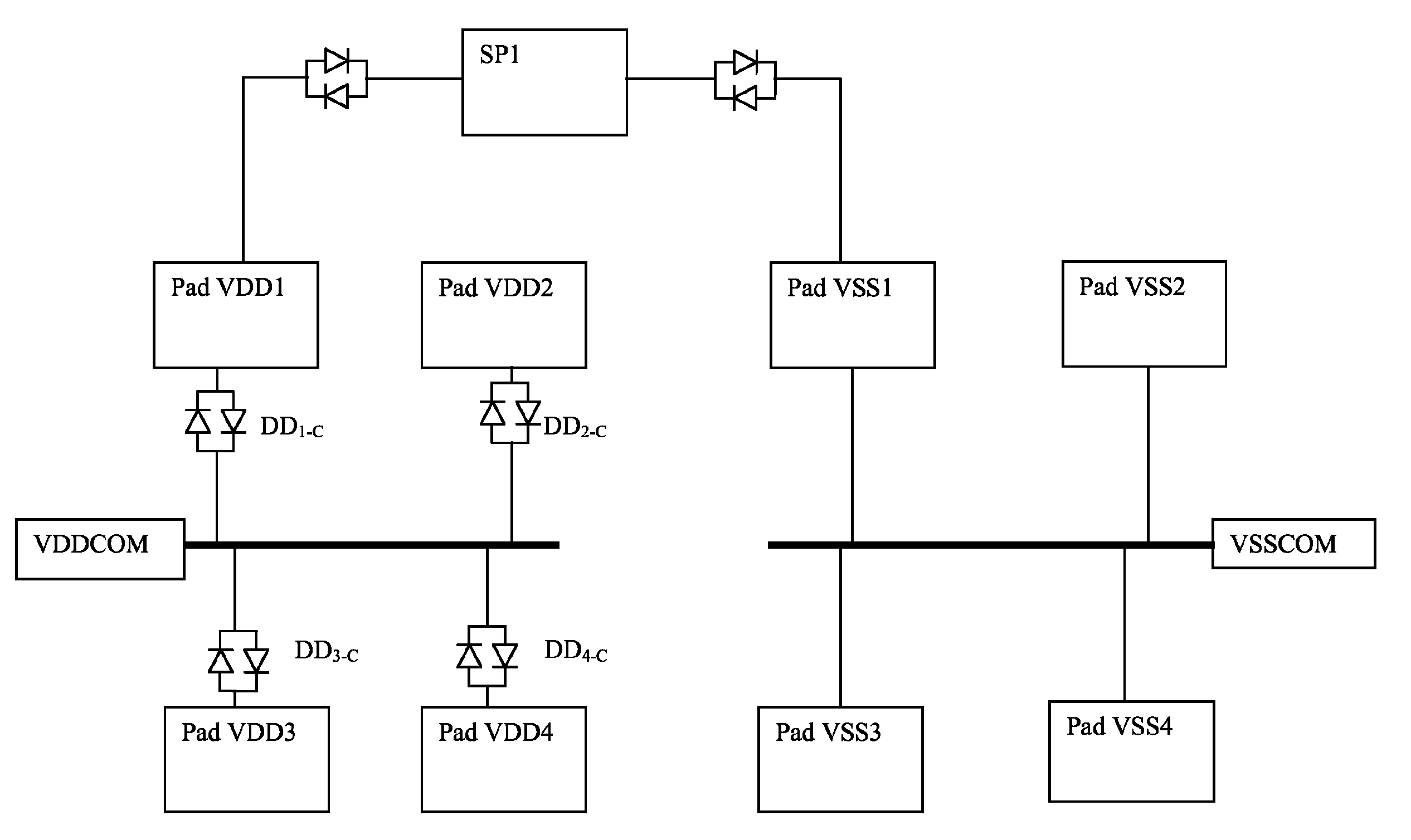
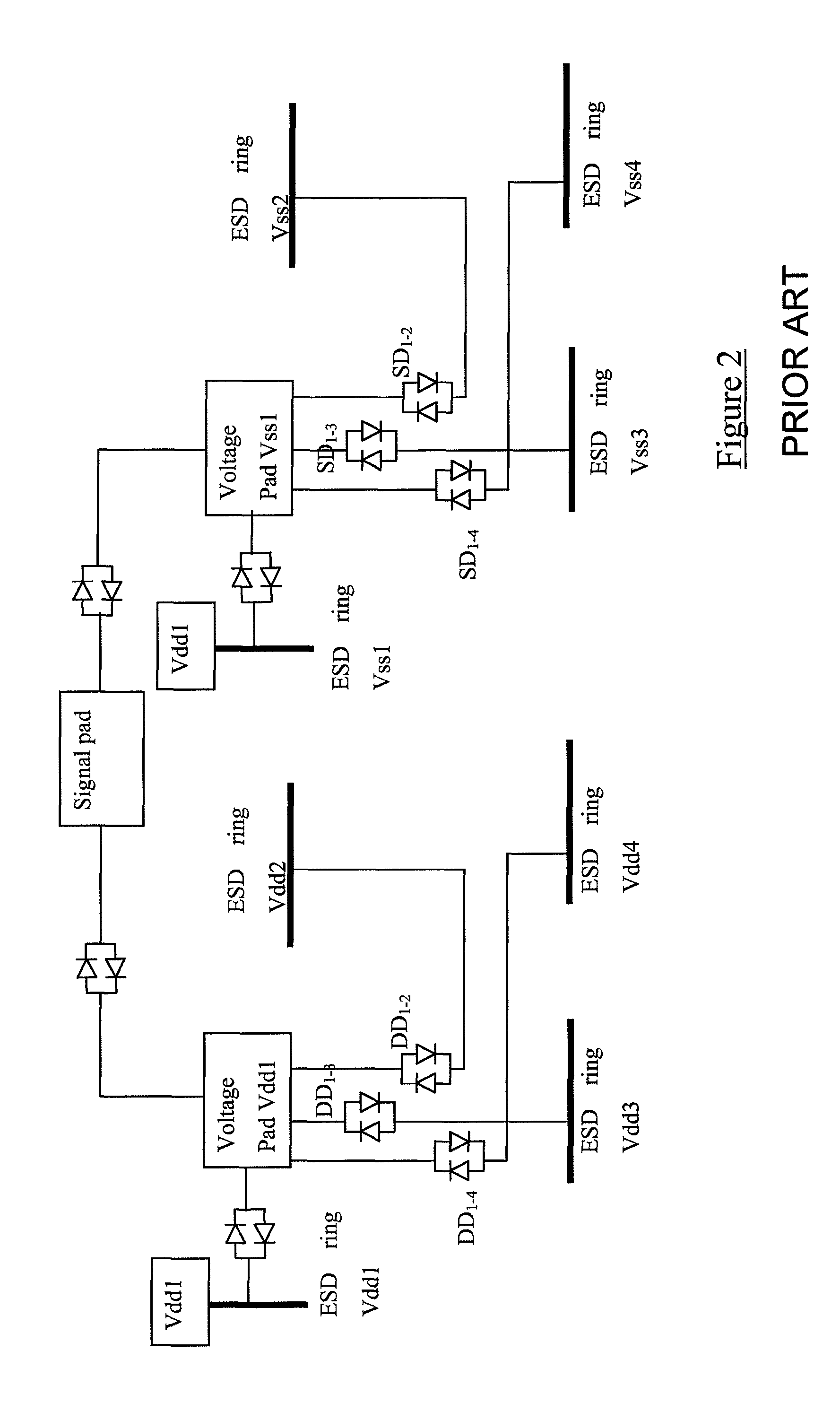
[0011]It is an advantage of at least certain embodiment of the invention that, in comparison with the known circuits discussed above, only a single ESD voltage supply and negative (e.g. ground) rail are required. This enables the IC to be constructed with fewer components and connections, thus minimising the physical size thereof, and reducing the electrical connection complexity. There is also no need to provide protective circuitry between each and every pair of supply pads—as in the known example. Furthermore, connecting all negative (ground) pads to a common ground rail avoids the need for each ground pad to be connected to every other ground pad by way of additional protective circuitry.

Problems solved by technology

It is well known that electrostatic discharge (ESD) can present a problem in small-scale devices such as integrated circuits (ICs).
This is because in an IC having ground and supply pins and pads, an ESD spike on one pin / pad may destroy the entire chip.
The need for a pair of ESD protection rails for each unit of a SoC is a significant disadvantage.
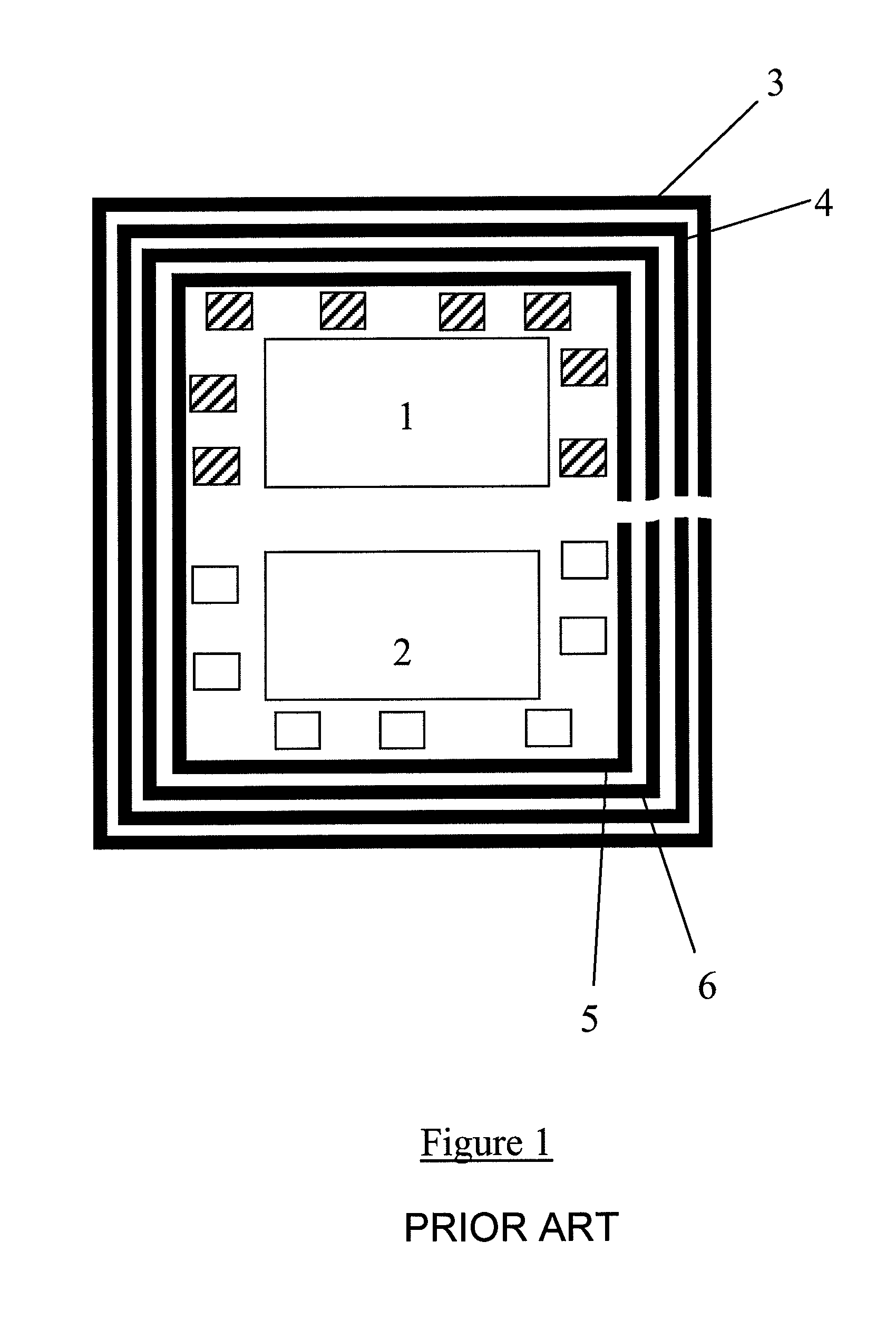
For example, an SoC having five internal blocks would require five pairs of ESD rings, which potentially increases the size of the chip and creates preferential breakdown mechanisms as some tracks may have lower ohmic paths than others (e.g. if connections are made with different lengths of wiring).
A further disadvantage is that the requirement for pairs of back-to-back diodes between each voltage supply pad and each and every other ESD protection ring of the same polarity necessitates a high number of diodes and circuitry connections on the chip, which again can increase the size of the chip and introduce further breakdown mechanisms.

Method used


Image

  • Electrostatic discharge protection circuit
  • Electrostatic discharge protection circuit
  • Electrostatic discharge protection circuit

Examples


Embodiment Construction

[0022]As has been described above, System on Chip (SoC) ESD protection circuits have in general relied upon the provision of a pair of peripherally extending ESD protection rings for each unit within the system, where each unit requires its own positive and negative supply voltages. These approaches have failed to recognise that for each polarity, a single ESD protection ring is sufficient, provided that ring is coupled to all of the supply voltage pads of that polarity.

[0023]Consider for example a four unit SoC IC, each unit requiring a positive supply voltage Vdd1 to Vdd4 and a negative supply voltage Vss 1 to Vss4. A first point to note is that the voltage supplies can be referenced to a single, common negative supply voltage, i.e. ground. As is illustrated schematically in FIG. 3, all of the negative supply pads of the four blocks are connected directly to a common “ground” ESD protection ring. This ring is in turn directly connected to a common Vss pad, “VSSCOM”, which is bonde...


PUM


Abstract

An integrated circuit having a plurality of circuit blocks, each block having one or more positive voltage supply pads, one or more negative voltage supply pads, and one or more signal pads. The integrated circuit further comprises an electrostatic protection circuit comprising a first electrostatic discharge protection rail for connection to a positive voltage supply point, a second electrostatic discharge protection rail for connection to a negative voltage supply point, and first protection circuitry coupling each said signal pad to both said first and second electrostatic discharge protection rails, the first protection circuitry being configured to provide a conduction path to one of the first and second rings in the event of an excessive voltage being present on one of said signal pads.

Description

CROSS REFERENCE TO RELATED APPLICATIONS[0001]This application claims the priority of PCT / GB2008 / 050568, filed on Jul. 14, 2008, which claims priority to Great Britain Application No. 0714703.6, filed Jul. 30, 2007, the entire contents of which are hereby incorporated in total by reference.TECHNICAL FIELD[0002]The present invention relates to an electrostatic discharge (ESD) protection circuit and, more particularly, to an ESD protection circuit for a System on Chip (SoC) susceptible to damage due to electrostatic discharge.BACKGROUND[0003]It is well known that electrostatic discharge (ESD) can present a problem in small-scale devices such as integrated circuits (ICs). This is because in an IC having ground and supply pins and pads, an ESD spike on one pin / pad may destroy the entire chip. A number of ways of addressing this problem have been suggested. It is known to provide an IC with circuitry which, in the event of an electrostatic discharge, forms a current discharge path for the...

Claims


Application Information

Patent Timeline
IPC IPC(8): H02H9/00
CPCH01L27/0251H01L27/0292H01L2924/0002H01L2924/00H01L23/60H01L27/0248
Inventor PADDEN, PAUL
Owner TOUMAZ TECH
Learn More