

Method of driving an active matrix electro-wetting on dielectric device and an active matrix electro-wetting on dielectric device
a dielectric device and active matrix technology, applied in the field of active matrix arrays, can solve the problem of not being able to actuate the array element in sufficient magnitude, and achieve the effect of reducing the physical size of the array element circuitry, reducing the minimum achievable size of the array element electrode 38, and improving manufacturing yield
- Summary
- Abstract
- Description
- Claims
- Application Information
AI Technical Summary
Benefits of technology
Problems solved by technology
Method used
Image

Examples
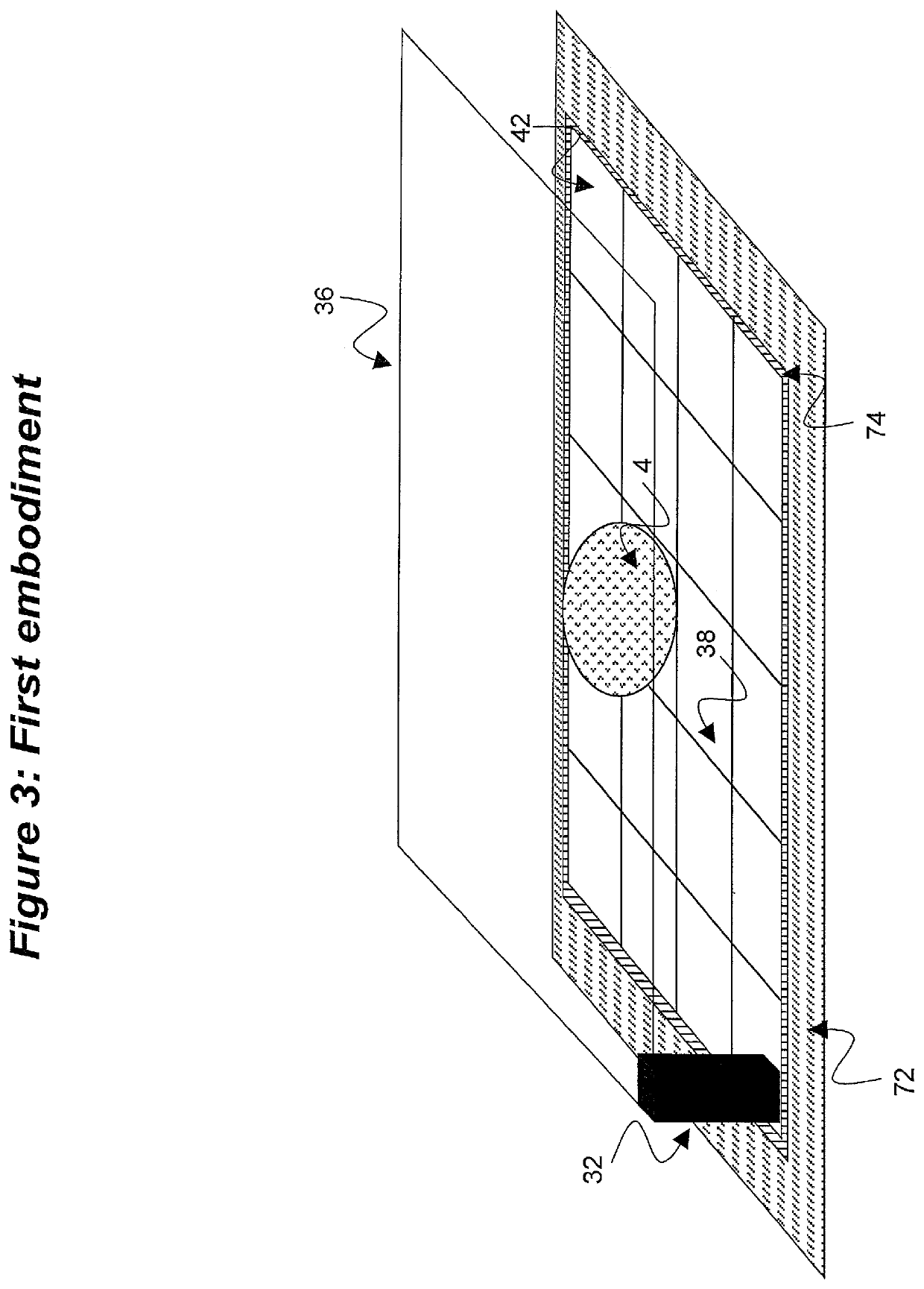
first embodiment
[0062]According to the invention, the actuation voltages at each array element of the AM-EWOD device are controlled by means of a “multi-frame-AC” method of driving. In summary each unique frame of data (F1) is written and re-written N times. The voltage signal on VTOP is then inverted and the inverse data frame (F1B) is then written and re-written N times. The process is then repeated for the next frame of data (F2 and then F2B).
[0063]In detail this method of driving is described as follows, with reference to FIG. 7 which shows a graphical representation of the timing signals supplied to the input data line DATA and to the top substrate electrode 28, and with reference to FIG. 8 whereby a graphical representation of exemplary data written to a whole or a part of the array is shown. In FIG. 8, a frame of data is denoted as a 2-dimensional array of squares, and a “1” or a “0” is shown in each array element to denote array elements written to either +0.5×VEW (programmed to “1”) or −0....
second embodiment
[0086]The arrangement of data frames according to the operation of the device according to the invention is shown in FIG. 9. The first frame of data F1 is written N times with the top substrate electrode 28 at a first reference potential, for example −0.5×VEW. (FIG. 9A). The potential of the top substrate electrode 28 is then set to a second reference potential, for example +0.5×VEW and the inverse data of data frame 2, F2B is written to the array (FIG. 9B). The potential of the top substrate electrode 28 is then set to the first reference potential, in this example −0.5×VEW and the data of data frame 3, F3 is written to the array (FIG. 9C). The potential of the top substrate electrode 28 is then set to the second reference potential, in this example +0.5×VEW and the inverse data of data frame 4, F4B is written to the array (FIG. 9D), and so on. That is, rather than each frame of data being written multiple times normal and multiple times inverted as in the method of FIG. 1, each fr...
third embodiment
[0090]An advantage of the invention is by only needing to write the frame of data once, the power consumption of the device is considerably reduced.
[0091]The third embodiment has been described for the case whereby the hold time t is identical for the operations immediately following frame F1 and frame F1B. Optionally, this need not be the case and where the hold time following frame F1 is t, then the hold time following frame F1B may be longer or may be shorter than t, without substantially affecting the performance of the device. Similarly the actuation potential of the positive and negative frames may be different.
[0092]It will be readily apparent that a combination of the second and third embodiments could also be realized by means of a small change to the timing schematics of FIG. 10, for example by making Frame 2 contain the DATA for F2B and frame 3 the data for F3, etc.
PUM
| Property | Measurement | Unit |
|---|---|---|
| actuation voltages | aaaaa | aaaaa |
| electro-wetting voltage | aaaaa | aaaaa |
| actuation voltage | aaaaa | aaaaa |
Abstract
Description
Claims
Application Information