

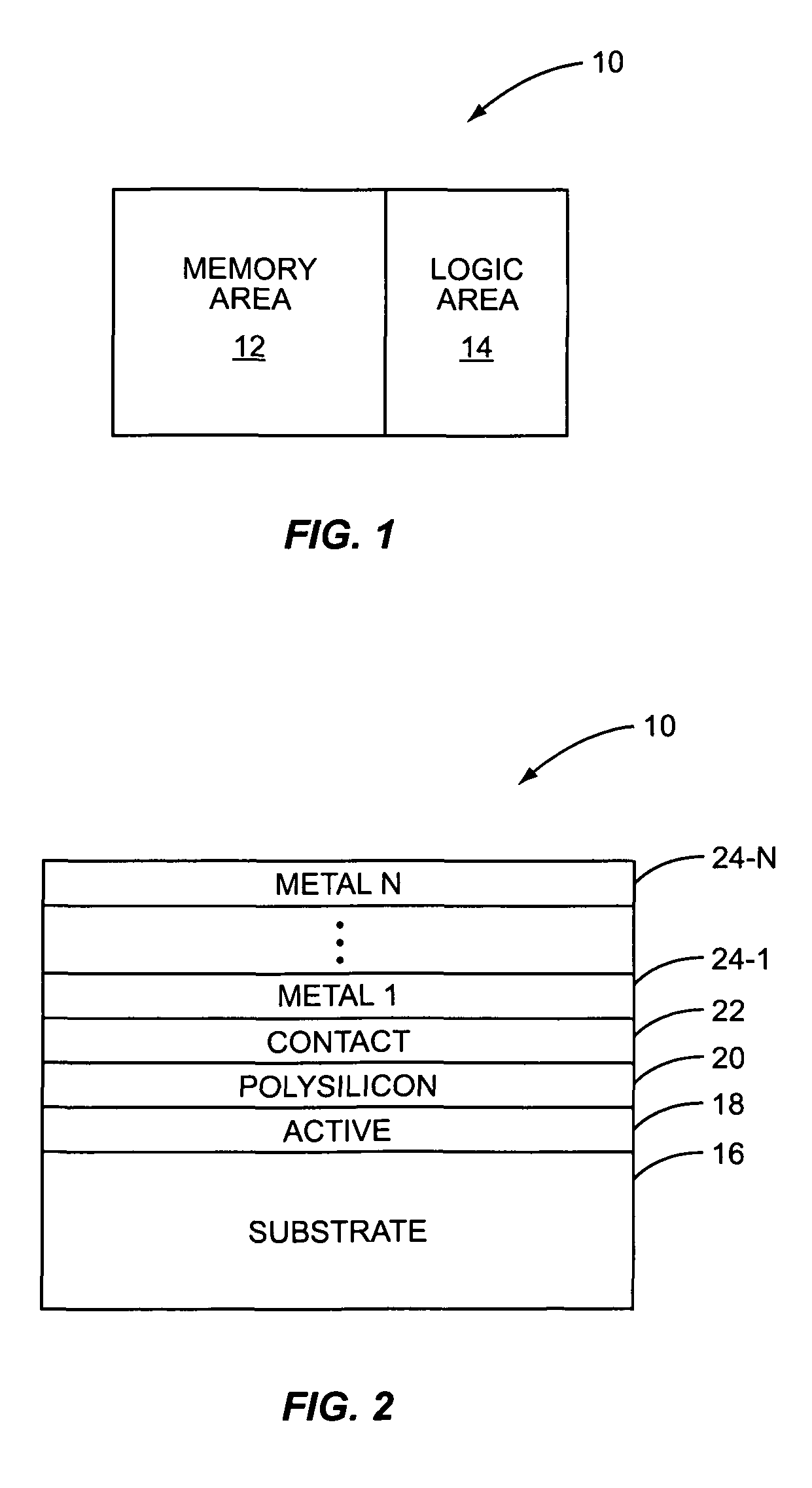
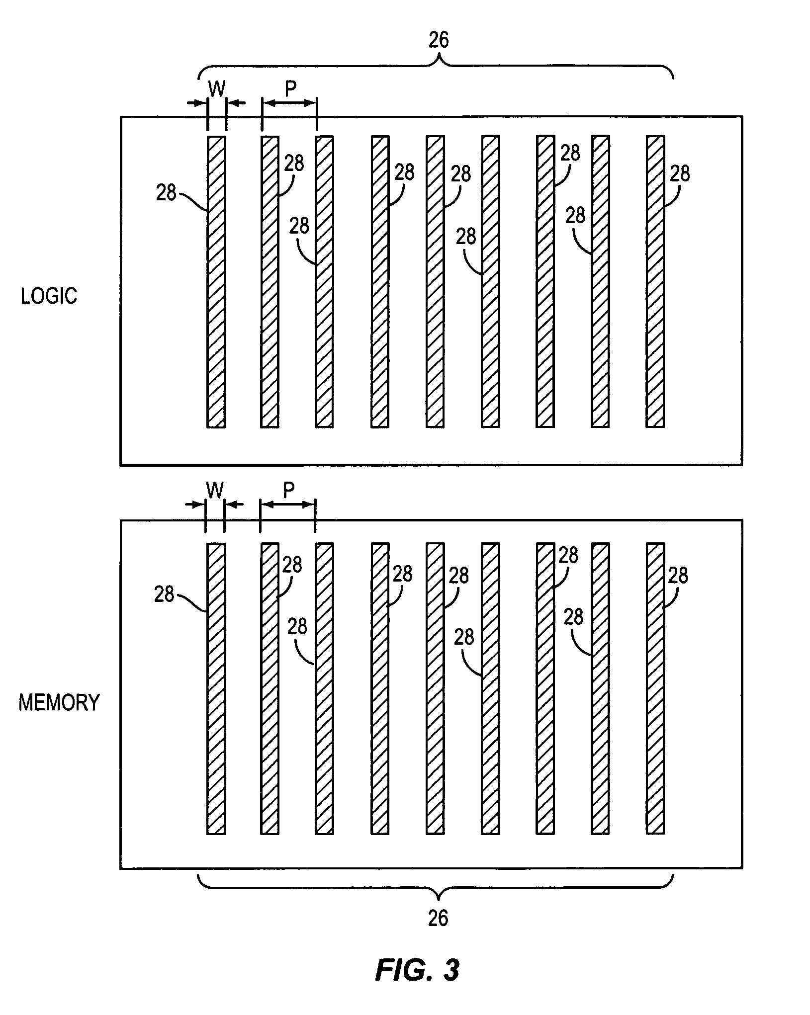
Regular pattern arrays for memory and logic on a semiconductor substrate
a semiconductor substrate and memory technology, applied in the field of integrated circuits, can solve the problems of systematic variability, lithographic process window, and inability to reproduce arbitrary layout patterns, and achieve the effect of reliable and affordably manufactured
- Summary
- Abstract
- Description
- Claims
- Application Information
AI Technical Summary
Benefits of technology
Problems solved by technology
Method used
Image

Examples
first embodiment
[0014]FIG. 6 is a flow chart for a process of fabricating an integrated circuit using a common grating pattern for memory and logic according to this disclosure;
[0015]FIGS. 7A through 7G graphically illustrate the process of FIG. 6 for exemplary memory and logic;
second embodiment
[0016]FIG. 8 is a flow chart for a process of fabricating an integrated circuit using a common grating pattern for memory and logic according to this disclosure;
[0017]FIGS. 9A through 9C graphically illustrate the process of FIG. 8 for exemplary memory and logic;
third embodiment
[0018]FIG. 10 is a flow chart for a process of fabricating an integrated circuit using a common grating pattern for memory and logic according to this disclosure;
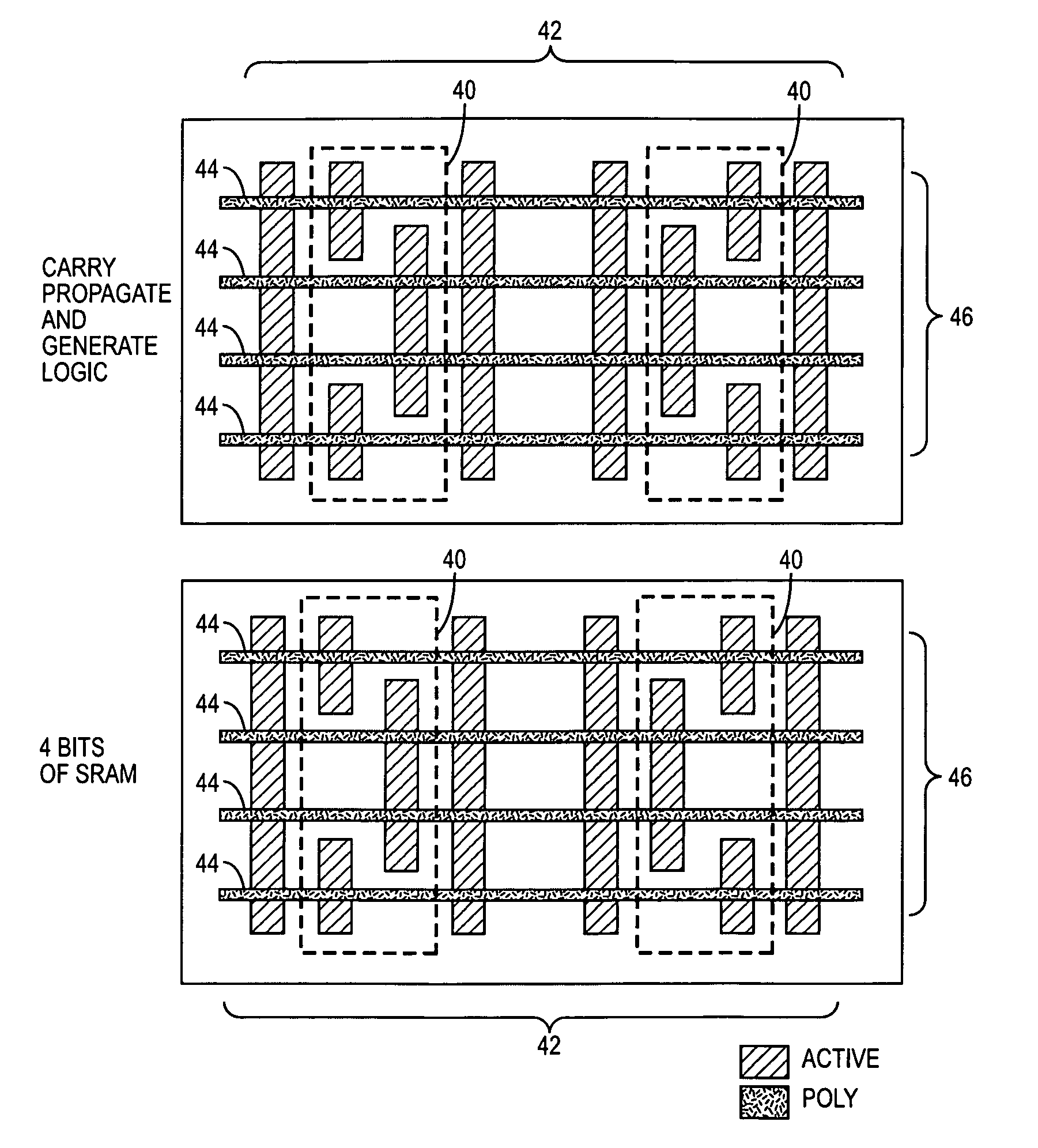
[0019]FIGS. 11A and 11B graphically illustrate the process of FIG. 10 for exemplary memory and logic having a common active layer pattern according to one embodiment of this disclosure;
[0020]FIGS. 12A and 12B graphically illustrate the process of FIG. 10 for exemplary memory and logic having different active layer patterns according to another embodiment of this disclosure; and
[0021]FIGS. 13A and 13B illustrate a diffusion breaking dummy transistor according to one embodiment of this disclosure.
PUM
 Abstract
Description
Claims
Application Information