
System on chip including an image processing memory with multiple access

a technology of image processing and system, applied in the field of system on the chip, can solve the problems of significant degrading of system performance, access to external memory, etc., and achieve the effects of reducing the incidence of accessing external memory, reducing the operation time, and improving system performan

Active Publication Date: 2012-06-12
SAMSUNG ELECTRONICS CO LTD
View PDF10 Cites 23 Cited by
  • Summary
  • Abstract
  • Description
  • Claims
  • Application Information

AI Technical Summary

Benefits of technology

The present invention relates to a system on chip (SoC) that includes an image processing logic block, a system bus, and a power supply unit. The image processing logic block performs image processing tasks and is connected to the system bus. The image memory interface is connected to the system bus and the image processing logic block. The image memory interface controls the paths for accessing the image processing memory block. The sub-systems in the SoC can access the image processing memory block through the system bus and the image memory interface. The power supply unit supplies power to the sub-systems and the image processing logic block. The invention improves the performance of the SoC by reducing the load on the external memory controller and reducing the incidence of accessing external memory.

Problems solved by technology

The access to the external memory significantly degrades performance of the system because a path for accessing to the external memory is typically heavily loaded.

Method used


Image

  • System on chip including an image processing memory with multiple access
  • System on chip including an image processing memory with multiple access
  • System on chip including an image processing memory with multiple access

Examples


Embodiment Construction

[0042]Embodiments of the present invention now will be described more fully with reference to the accompanying drawings, in which embodiments of the invention are shown. This invention may, however, be embodied in many different forms and should not be construed as limited to embodiments set forth herein. Rather, embodiments are provided so that this disclosure will be thorough and complete, and will fully convey the scope of the invention to those skilled in the art. Like reference numerals refer to like elements throughout this application.

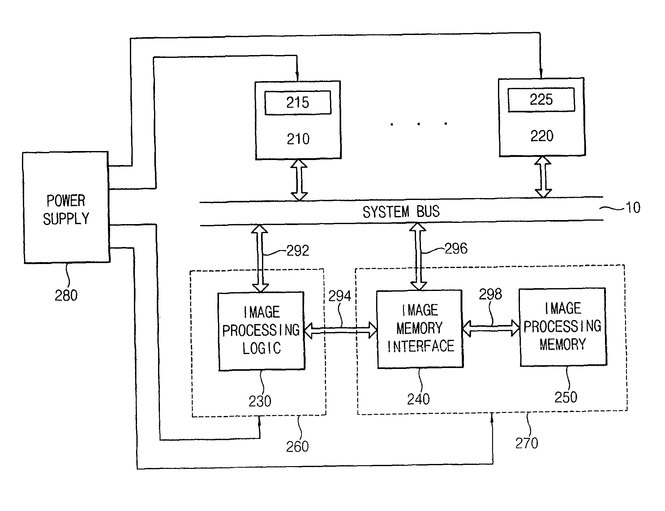
[0043]FIG. 4 is a block diagram illustrating a system on chip including an image processing memory with multiple access according to an exemplary embodiment of the present invention.

[0044]Referring to FIG. 4, a system on chip includes a system bus 10, a plurality of sub-systems 110 and 120 connected to the system bus 10, an image processing logic block 130 connected to the system bus 10, an image processing memory block 150 and an image memory i...


PUM


Abstract

A system on chip (Soc) includes a system bus, a plurality of sub-systems, an image processing logic block, an image memory interface and an image processing memory block. The sub-systems are respectively connected to the system bus. The image processing logic block is connected to the system bus. The image processing logic block performs an image processing. The image processing logic block is included in a first power domain. The image memory interface is connected to the system bus and the image processing logic block. The image processing memory block is connected to the image memory interface. The image processing memory block is used for the image processing. The image memory interface and the image processing memory block are included in a second power domain different from the first power domain.

Description

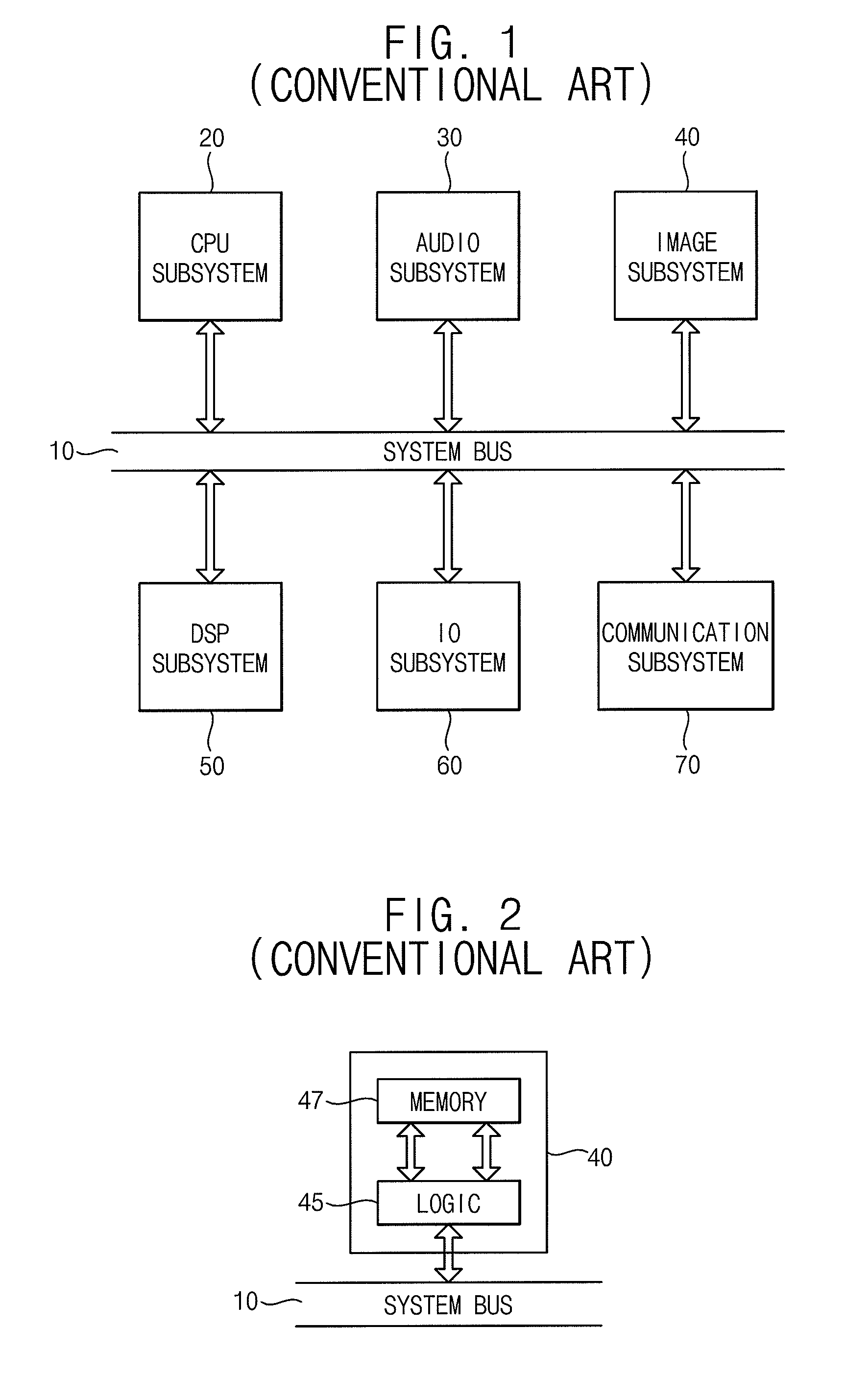
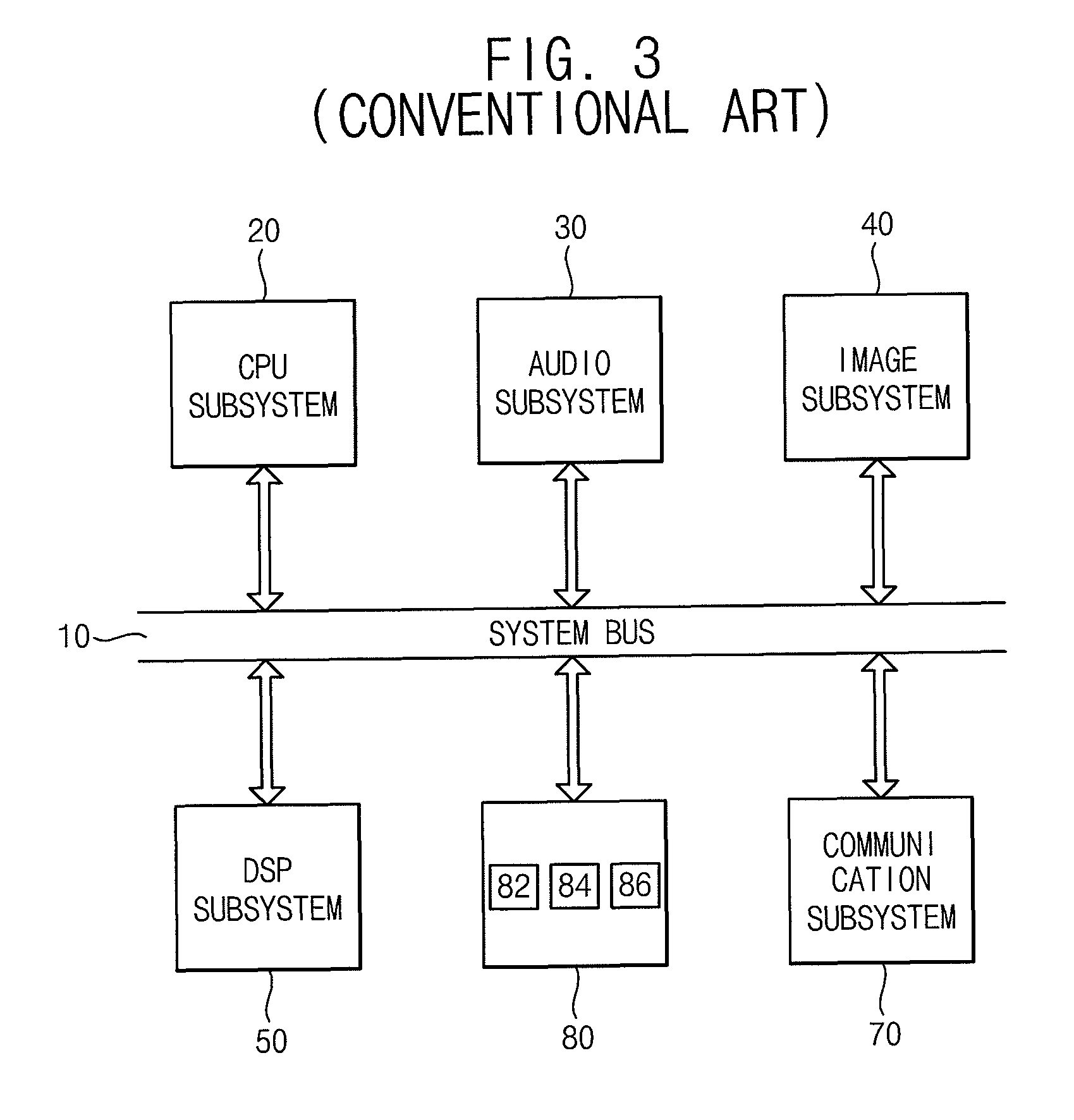
CROSS-REFERENCE TO RELATED APPLICATIONS[0001]This application claims priority under 35 USC §119 to Korean Patent Application No. 2007-11895 filed on Feb. 6, 2007 in the Korean Intellectual Property Office (KIPO), the disclosure of which is incorporated herein in its entirety by reference.BACKGROUND OF THE INVENTION[0002]1. Field of the Invention[0003]The present invention relates to a system on chip, and more particularly to a system on chip including an image processing memory with multiple access.[0004]2. Description of Related Art[0005]Sub-systems in a conventional system on chip may be divided into a plurality of power domains, and the sub-systems in the respective power domains may be powered individually.[0006]FIG. 1 is a block diagram illustrating a conventional system on chip including a plurality of sub-systems.[0007]Referring to FIG. 1, the conventional system on chip includes a plurality of sub-systems. Each of the sub-systems includes a central processing unit (CPU) sub-...

Claims


Application Information

Patent Timeline
Patent Type & Authority Patents(United States)
IPC IPC(8): G06F13/14G09G5/39
CPCG06T1/20G06F12/00G06F13/14G06F15/76G06F15/78
Inventor PARK, SUN-HEEKANG, SHIN-CHAN
Owner SAMSUNG ELECTRONICS CO LTD
Learn More