Shift register receiving all-on signal and display device

a technology of display device and shift register, which is applied in the field of shift register and display device, can solve the problems of increased power consumption, increased area for laying clock wires, viewers experiencing discomfort, etc., and achieve the effect of reducing the load on the all-on control signal line, and restoring to normal operation more quickly

Inactive Publication Date: 2012-07-17
SHARP KK
View PDF18 Cites 17 Cited by
  • Summary
  • Abstract
  • Description
  • Claims
  • Application Information

AI Technical Summary

Benefits of technology

[0057]According to the first aspect of the invention, when the active all-on control signal is provided to the unit circuit, the first output signal generation circuit stops outputting the on-voltage as the first output signal at the same time as the all-on output signal generation circuit outputs the on-voltage to the first output terminal as the first output signal. Also, the second output signal generation circuit outputs the off-voltage to the second output terminal as the second output signal. In this manner, during all-on operation, the shift register can output the on-voltage to the first output terminal as the first output signal and the off-voltage to the second output terminal as the second output signal.
[0058]According to the second aspect of the invention, when the active all-on control signal is provided to the unit circuit, the first output control transistor, the second output control transistor, and the first output reset transistor are brought into off-state. On the other hand, the second output reset transistor and the third output control transistor are brought into on-state. As a result, when the shift register performs all-on operation, no through-current flows from the third output control transistor to the first output reset transistor. Also, regardless of the levels of the clock signals, no through-current flows from the third output control transistor to the first output control transistor. Furthermore, the all-on control signal is provided to the control terminal of the third output control transistor, and therefore all-on control terminals are not directly connected to any external circuit. Thus, load on the all-on control signal lines can be reduced. Also, during normal operation, when the first output reset transistor is brought into on-state, the same off-voltage is provided to the second conducting terminal and the control terminal of the first output control transistor. At this time, no potential difference occurs between the second conducting terminal and the control terminal of the first output control transistor even when the value of the off-voltage varies due to the power circuit being affected by noise, and therefore the first output control transistor is not brought into on-state. Thus, no through-current flows from the first output control transistor to the first output reset transistor.
[0059]According to the third aspect of the invention, when the all-on control signal is provided to the control terminal of the reset signal output transistor, the reset signal output transistor provides the on-voltage to the control terminal of the second output reset transistor as the reset signal. On the other hand, the discharge circuit provides an off-voltage to the control terminals of the first and second output control transistors while the reset signal is an on-voltage. Therefore, when the all-on control signal is provided to the unit circuit, the second output reset transistor is brought into on-state, so that the off-voltage is outputted to the second output terminal as the second output signal, and the first and second output control transistors are brought into off-state, so that the first output signal is stopped from being outputted. In addition, the all-on control signal is also provided to the control terminal of the reset signal output transistor, and therefore all-on control terminals are not directly connected to any external circuit. Thus, load on the all-on control signal lines can be reduced.
[0060]According to the fourth aspect of the invention, in order not to provide the on-voltage, which is outputted by the reset signal generation circuit as the reset signal, to the control terminal of the first output reset transistor, the reset signal block transistor shuts off the reset signal generation circuit and the control terminal of the first output reset transistor. The off-voltage supply transistor provides an off-voltage to the control terminal of the first output reset transistor. Also, the discharge circuit provides an off-voltage to the control terminals of the first and second output control transistors while the reset signal is an on-voltage. Therefore, during all-on operation, the first output control transistor, the second output control transistor, and the first output reset transistor can be stopped from outputting the first or second output signal. Also, when returning from all-on operation to normal operation, an on-voltage is provided to the control terminal of the reset signal block transistor, and an off-voltage is provided to the control terminal of the off-voltage supply transistor. As a result, the first output reset transistor is brought into on-state, so that the off-voltage is outputted to the first output terminal as the first output signal. Thus, when returning from all-on operation to normal operation, the shift register can return to normal operation more quickly because it is not necessary to perform initialization operation.
[0061]According to the fifth aspect of the invention, when the active all-on control signal is provided, the input signal control circuit blocks an input signal from a previous-stage unit circuit, and provides an off-voltage for an input terminal for receiving the input signal. Thus, the shift register can perform all-on operation regardless of the level of the input signal from the previous-stage unit circuit.
[0062]According to the sixth aspect of the invention, when the second clock signal is provided to the control terminal of the first transistor, thereby bringing the first transistor into on-state, the reset signal generation circuit can cause the reset signal to quickly rise from the off-voltage to the on-voltage.

Problems solved by technology

Also, increasing the number of clock signals to be provided to the shift register results in an increased area for laying out clock wires and increased power consumption.
When such a shift register is used in a liquid crystal display device, video disturbance caused by turning on or off the power circuit of the liquid crystal display device might be visible to the human eye, so that viewers experience a feeling of discomfort.

Method used


Image

  • Shift register receiving all-on signal and display device
  • Shift register receiving all-on signal and display device
  • Shift register receiving all-on signal and display device

Examples


first embodiment

[0101]

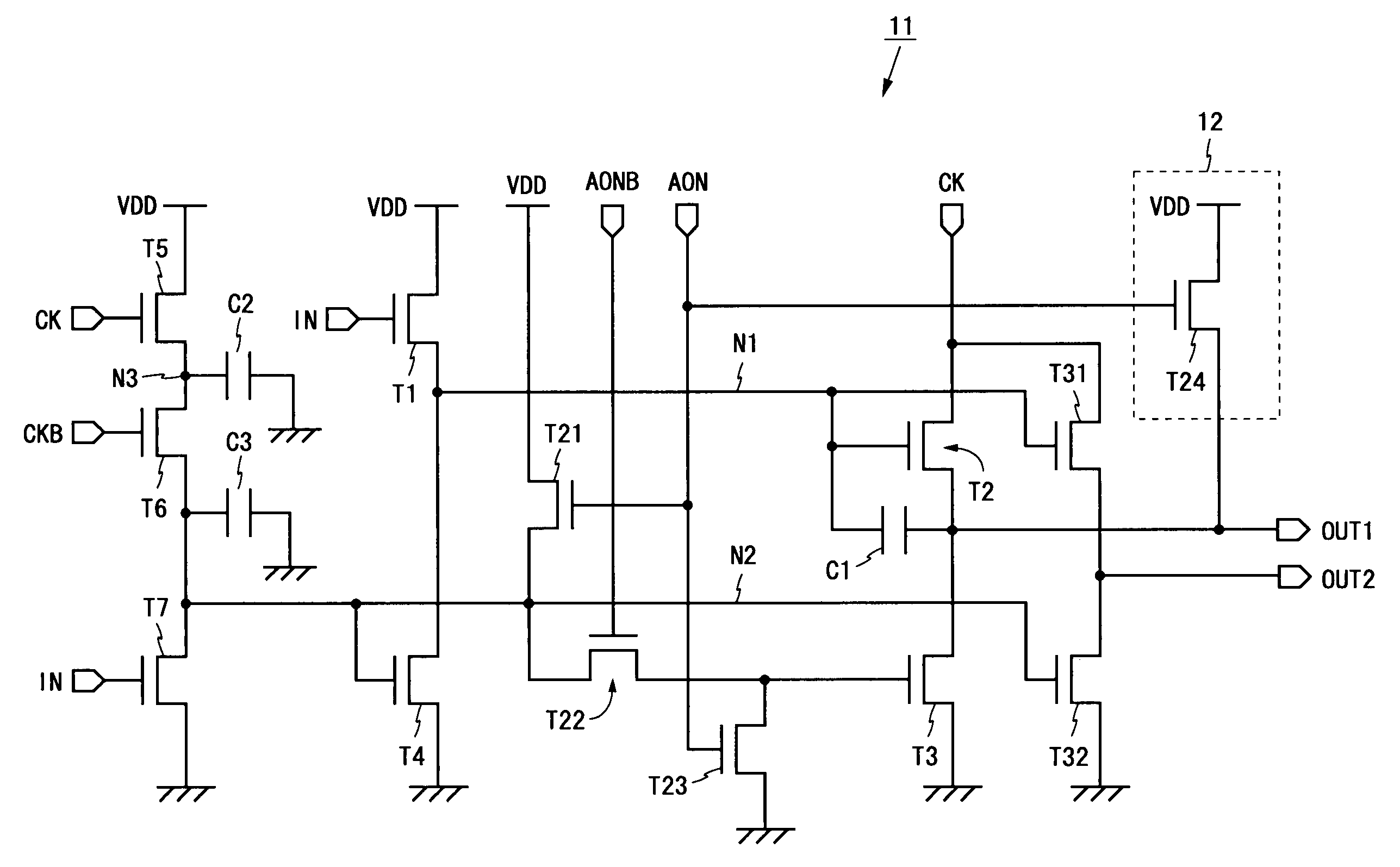
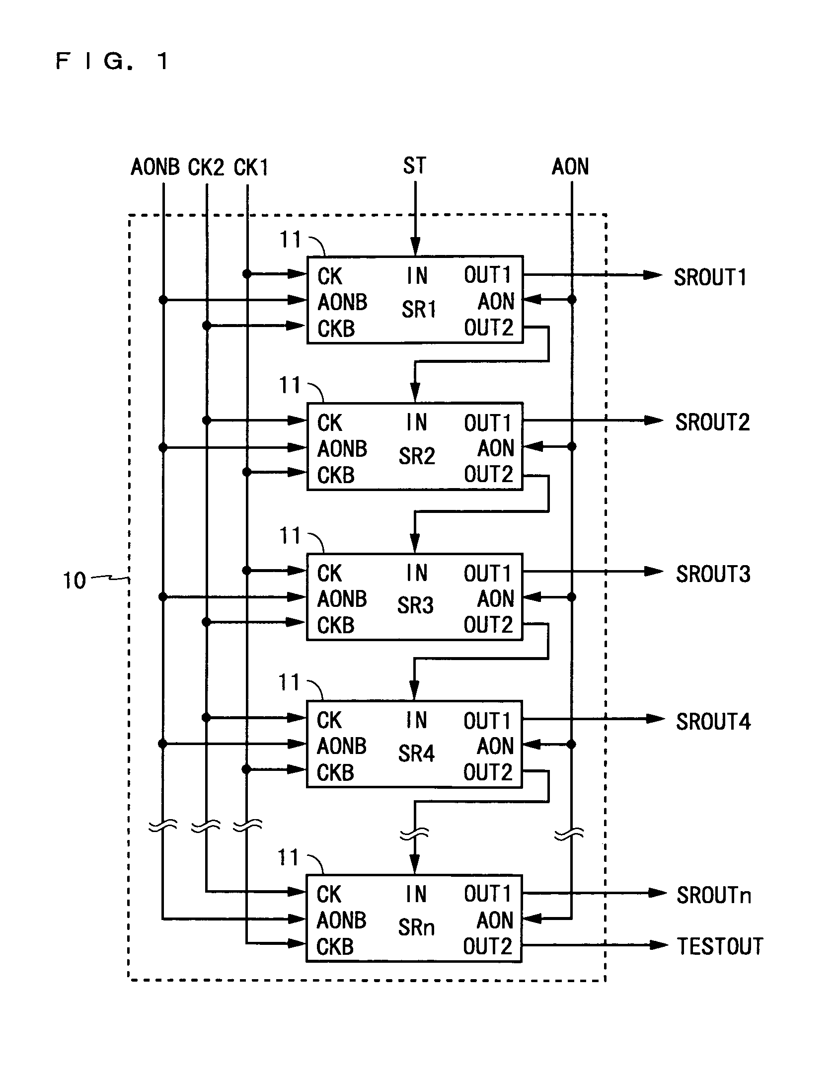
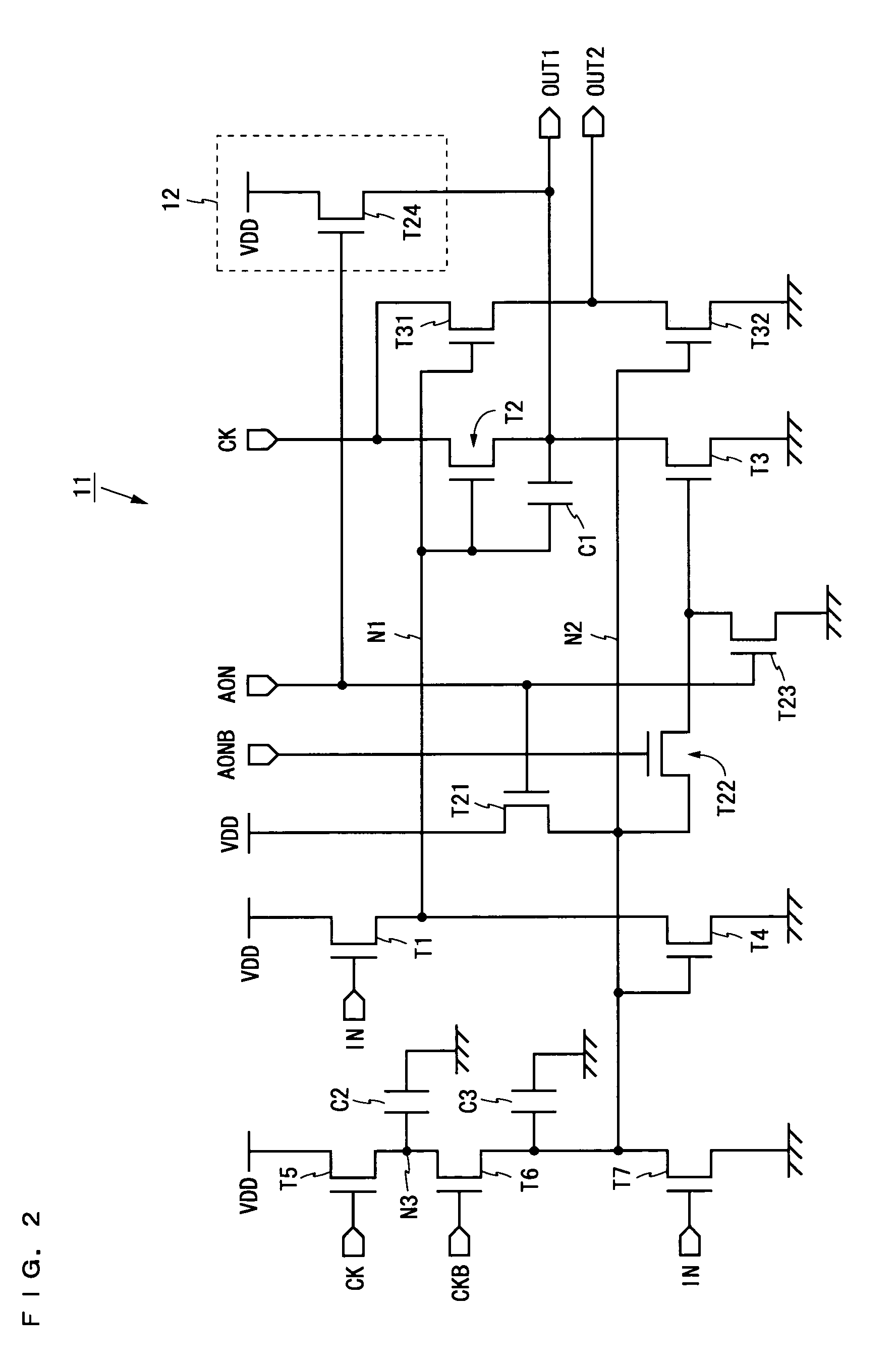
[0102]FIG. 1 is a block diagram illustrating the configuration of a shift register 10 according to a first embodiment of the present invention. The shift register 10 shown in FIG. 1 is configured by connecting n (where n is an integer of 2 or more) unit circuits 11 in multiple stages. Each of the unit circuits 11 has clock terminals CK and CKB, an input terminal IN, a first output terminal OUT1, a second output terminal OUT2, and all-on control terminals AON and AONB. Hereinafter, a signal which is inputted / outputted via a terminal is referred to by the same name as that terminal (e.g., a signal which is inputted via the clock terminal CK is referred to as a clock signal CK).

[0103]The shift register 10 is externally supplied with a start pulse ST, two-phase clock signals CK1 and CK2, and all-on control signals AON and AONB (negation to AON). The start pulse ST is provided to the input terminal IN of the first-stage unit circuit 11. The clock signal CK1 is provided to the clock...

second embodiment

[0141]

[0142]The shift register according to the second embodiment of the present invention is configured in the same manner as the shift register 10, and therefore its block diagram and description are omitted.

[0143]FIG. 6 is a circuit diagram of a unit circuit 21 included in the shift register. Elements of the unit circuit 21 which correspond to those of the unit circuit 11 shown in FIG. 2 are denoted by the same reference characters and any descriptions thereof will be omitted. The unit circuit 21 has two input circuits, i.e., transistors T1 and T7, as provided in the unit circuit 11, and these transistors are connected at their gate terminals to an output terminal of an input signal control circuit 22.

[0144]The input signal control circuit 22 includes two N-channel transistors T41 and T42, and the transistor T41 is connected at a drain terminal to an input terminal IN and at a gate terminal to an all-on control terminal AONB. Also, the transistor T42 is connected at a gate termin...

third embodiment

[0150]

[0151]The shift register according to the third embodiment of the present invention is configured in the same manner as the shift register 10, and therefore its block diagram and description will be omitted.

[0152]FIG. 8 is a circuit diagram of a unit circuit 31 included in the shift register. Elements of the unit circuit 31 which correspond to those of the unit circuit 11 shown in FIG. 2 are denoted by the same reference characters, and any descriptions thereof will be omitted. The unit circuit 31 is provided with a reset signal generation circuit 32 partially different in configuration from the reset signal generation circuit provided in the unit circuit 11.

[0153]The reset signal generation circuit 32 differs from the reset generation circuit of FIG. 1, in that a resistive element R1 is provided in place of the transistor T5, and the capacitative element C2 is omitted. Therefore, in the case of the reset signal generation circuit 32, when the clock signal CKB is set to high l...


PUM


Abstract

At least one embodiment of the present invention is directed to, even when external noise is applied to a shift register during all-on operation, preventing through-current from flowing in unit circuits and also to prevent increase in load on all-on control signal lines. When a high-level all-on control signal is provided to a unit circuit of a shift register, a transistor T3 is brought into off-state, so that a transistor T2 cannot output an on-voltage to a first output terminal. However, a transistor T24 is brought into on-state, so that the first output terminal outputs an on-voltage to the exterior. On the other hand, a transistor T32 is brought into on-state, so that a second output terminal outputs an off-voltage to a unit circuit 11 in the next stage. At this time, the transistor T3 is kept in off-state, so that no through-current flows to the transistors T24 and T3.

Description

TECHNICAL FIELD[0001]The present invention relates to shift registers and display devices, and particularly the invention relates to a shift register preferably used for a driver circuit of a display device or an imaging device as well as to a display device or an imaging device using such a shift register.BACKGROUND ART[0002]Active-matrix display devices display video by selecting two-dimensionally arranged display elements row by row, and writing a voltage to the selected display elements in accordance with data to be displayed. To select display elements row by row, a shift register for sequentially shifting output signals based on clock signals is used as a scanning signal line driver circuit. Also, as for display devices in which dot-sequential drive is performed, a similar shift register is provided in a data signal line driver circuit.[0003]For some liquid crystal display devices, a production process intended to form TFTs (Thin Film Transistors) in display elements is used f...

Claims


Application Information

Patent Timeline
Patent Type & Authority Patents(United States)
IPC IPC(8): G09G3/36G09G5/00G06F3/038
CPCG09G3/20G09G3/3266G09G3/3275G09G3/3648G09G3/3674G09G3/3677G09G3/3685G11C19/28G09G3/3688G09G2300/0426G09G2310/0245G09G2310/0267G09G2310/0275G09G2310/0286G09G2310/0291
Inventor OHKAWA, HIROYUKIFURUTA, SHIGESASAKI, YASUSHIMURAKAMI, YUHICHIROH
Owner SHARP KK
Why Eureka
Try Eureka