Integrated Doherty amplifier

a doherty amplifier and integrated technology, applied in amplifier combinations, amplifiers with min 3 electrodes or 2 pn junctions, solid-state devices, etc., can solve the problems of parasitic capacitance, signal loss, parasitic capacitance, etc., to achieve the effect of large choke inductance, low impedance, and relaxed requirements

Active Publication Date: 2012-07-24
AMPLEON NETHERLANDS
View PDF11 Cites 22 Cited by
  • Summary
  • Abstract
  • Description
  • Claims
  • Application Information

AI Technical Summary

Benefits of technology

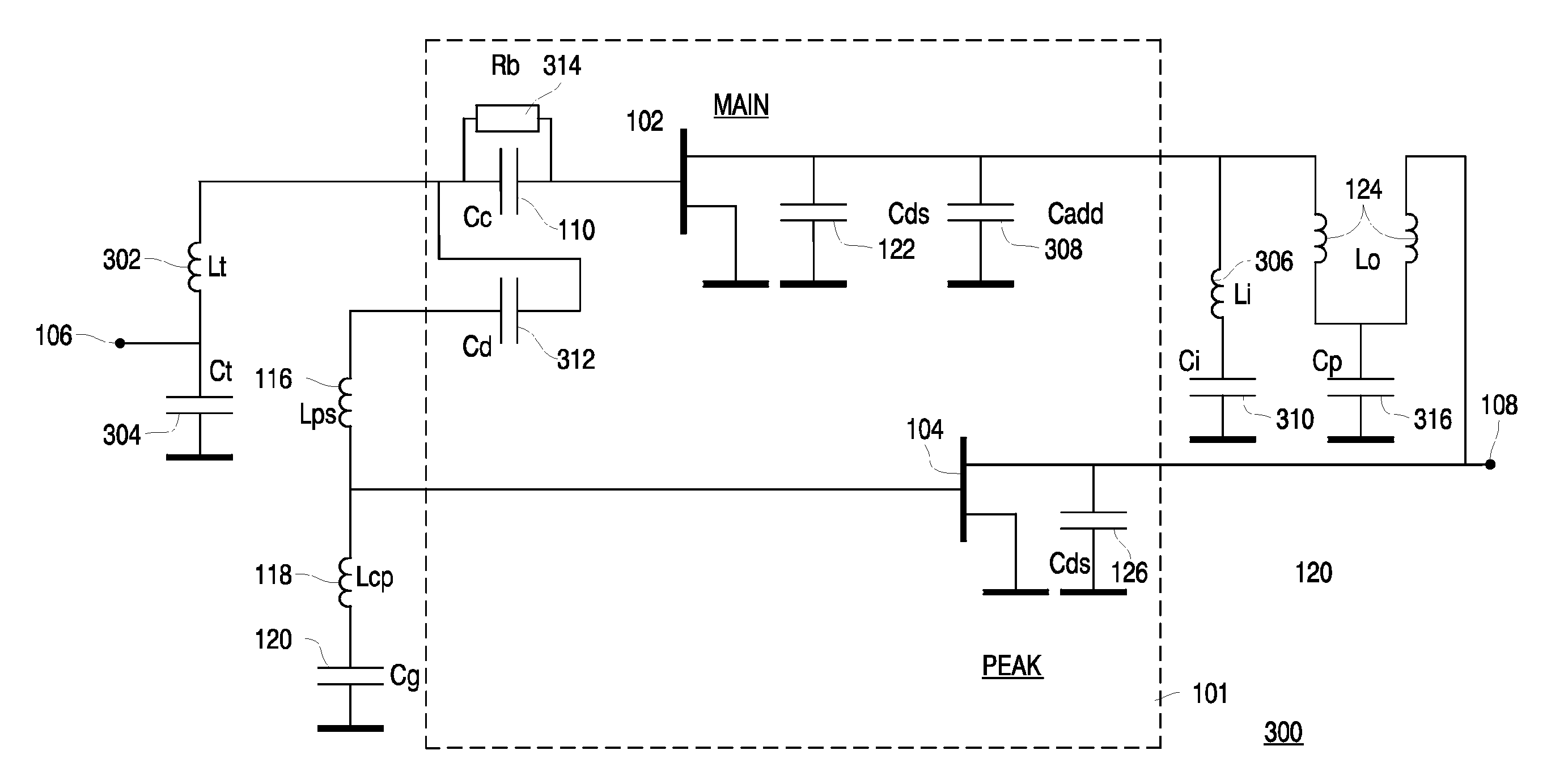
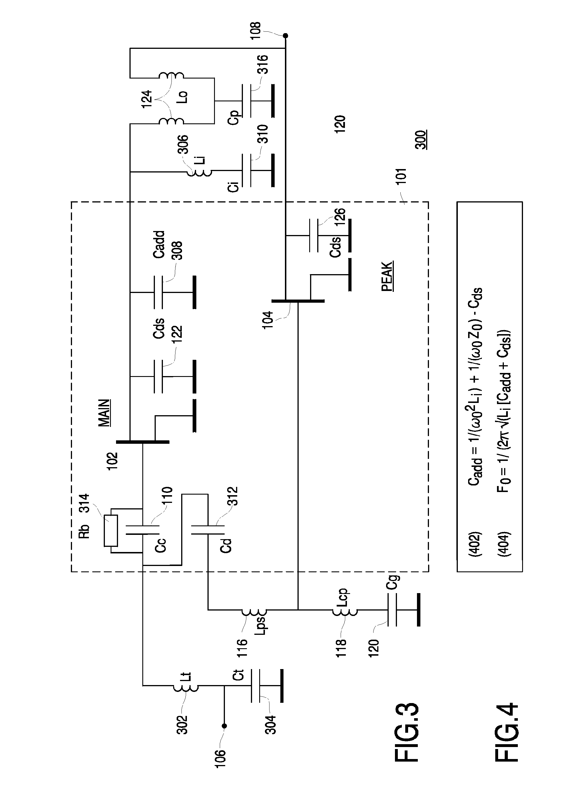
[0011]The inventor proposes the following approach to solving the problem. One measure is to modify the input network of the Doherty amplifier by removing some components from the active LDMOS die and put them onto another substrate, and / or to eliminate some components altogether, in order to free up space on the LDMOS die. This allows to decrease the loss of signal and to free up space on the LDMOS die so as to make the layout less dense. Another measure is to design the layout, bond wire arrangement, bond wire location, and bond wire orientation so as to reduce or eliminate the harmful electromagnetic coupling between components of the network.
[0019]A further design option relates to using a peak stage that is larger than the main stage. Another design option relates to making a large-scale Doherty device by having a plurality of Doherty amplifiers according to the invention arranged in parallel so as to form an array. The inputs of the Doherty amplifiers are combined at the input lead of the package and the output of the Doherty amplifiers are combined at the output lead of the package. This then enables to create an attractive amplifier device for use in high-power (e.g. 150 Watt) applications.

Problems solved by technology

A first consideration relates to the fact that the highly-doped silicon substrate used in LDMOS does not allow creating integrated high-quality inductances.
Such inductances introduce losses that directly affect the gain of an integrated Doherty amplifier.
A second consideration relates to the fact that bond pads, arranged on highly doped substrate, introduce parasitic capacitances and also signal losses.
So, if an inductance is needed where more than one bond wire is required with intermediate bond pads, then a non-desired impedance transformation or a phase-shift will occur, and also additional signal losses will be introduced in such an inductance.
As a result, the CLC transmission line and Doherty amplifier performance will degrade.
This constitutes a genuine challenge to the designer, as in general a Doherty amplifier requires many more components for its implementation than the traditional AB-class and A-class RF power devices.
On the other hand, the space or volume for accommodating the configuration is very limited, as a result of which a plurality of bonding wires, belonging to different parts of the Doherty amplifier and carrying different currents with arbitrary amplitudes and phases, are to be arranged close to one another.
This implies that these bonding wires will inevitably be coupled to each other by magnetic fields, thereby seriously hampering the Doherty operation.

Method used


Image

  • Integrated Doherty amplifier
  • Integrated Doherty amplifier
  • Integrated Doherty amplifier

Examples


Embodiment Construction

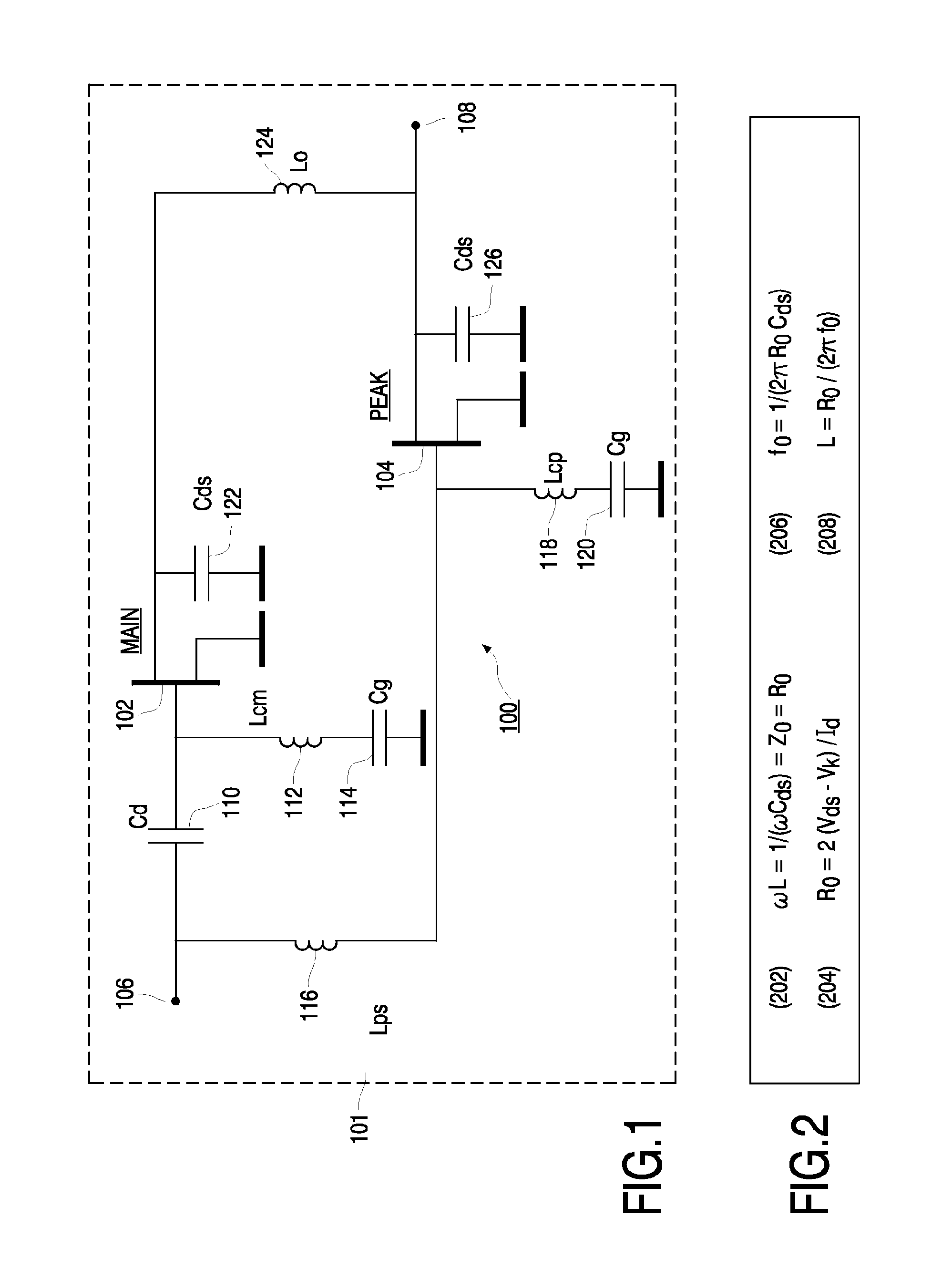
[0027]When modifying the design of cell 100 for operation in these other frequency ranges, the following should be taken into consideration. A first consideration relates to the fact that the highly-doped silicon substrate used in LDMOS does not allow creating integrated high-quality inductances. Typically, the best quality factor (Q-factor) of around 6 is attainable at a frequency of 2 GHz. At all other frequencies, above or below, the quality factor is lower. Such inductances in the input network introduce direct losses that directly affect the gain of an integrated Doherty amplifier. In the output network, such integrated inductances will also affect the gain, as well as power capability and efficiency.

[0028]A second consideration relates to the belief that an integrated Doherty amplifier device is going to be commercially successful only if the device outline is similar to that of traditional class-AB devices. That is, the integrated Doherty device is preferably to have a simila...


PUM


Abstract

The invention relates to an integrated Doherty amplifier with an input network connecting the input to the main stage and to the peak stage, and with an output network connecting the main stage and the peak stage to the output. The output network has a shunt capacitor to signal-ground in parallel to a parasitic capacitance of the main stage, and has a shunt inductor between the main stage and signal ground. The shunt configuration enables to use the MMIC Doherty amplifier in a wide frequency range. At least some of the inductors of the input network and / or output network are implemented using bond wires. Their orientations and locations provide minimal mutual electromagnetic coupling between the wires and the return RF current paths.

Description

FIELD OF THE INVENTION[0001]The invention relates to an electronic circuit with a Doherty amplifier.BACKGROUND ART[0002]As known, a classical Doherty amplifier has two amplifying devices arranged in parallel and of the same power capability. The first one of the devices (main stage) operates in a class-AB amplifier mode and the second one (peak stage) operates in a class-C amplifier mode. These devices are separated at their inputs and at their outputs by 90° phase-shifting networks. The output phase-shifting network has a specific characteristic impedance Z0 which must be equal to the optimal load impedance RLm of the main stage. The input signal is split so as to drive the two amplifiers, and a summing network, known as an “impedance inverter” or a “Doherty combiner”, is operative to: a) combine the two output signals, b) to correct for phase differences between the two output signals, and c) to provide an inverted impedance at the output of the Doherty amplifier with respect to t...

Claims


Application Information

Patent Timeline
Patent Type & Authority Patents(United States)
IPC IPC(8): H03F3/68
CPCH03F1/0288H03F3/195H01L2224/48137
Inventor BLEDNOV, IGOR
Owner AMPLEON NETHERLANDS
Why Eureka
Try Eureka