Resistor and method for making same

a resistor and metal strip technology, applied in the direction of resistor details, resistor housing/enclosement/embedding, resistors adapted for terminal application, etc., can solve the problems of nickel plating method limited to large sizes, nickel plating method limited to resistance measurement at laser trimming,

Active Publication Date: 2012-08-14
VISHAY DALE ELECTRONICS INC
View PDF13 Cites 16 Cited by
  • Summary
  • Abstract
  • Description
  • Claims
  • Application Information

AI Technical Summary

Benefits of technology

[0007]Therefore, it is a primary object, feature, or advantage of the present invention to improve over the state of the art and to provide a small sized low resistance value metal strip resistor and a method for making it.
[0008]According to one aspect of the present invention, a metal strip resistor is provided. The metal strip resistor includes a metal strip forming a resistive element and providing support for the metal strip resistor without use of a separate substrate. There are first and second opposite terminations overlaying the metal strip. There is plating on each of the first and second opposite terminations. There is also an insulating material overlaying the metal strip between the first and second opposite terminations.
[0009]According to another aspect of the present invention, a metal strip resistor is provided. The metal strip resistor includes a metal strip forming a resistive element and providing support for the metal strip resistor without use of a separate substrate. There are first and second opposite terminations sputtered directly to the metal strip. There is plating on each of the first and second opposite terminations. There is also an insulating material overlaying the metal strip between the first and second opposite terminations.
[0010]According to yet another aspect of the present invention, a metal strip resistor is provided. The resistor includes a metal strip forming a resistive element and providing support for the metal strip resistor without use of a separate substrate. There is an adhesion layer sputtered to the metal strip. There are first and second opposite terminations sputtered to the adhesion layer. There is plating on each of the first and second opposite terminations and an insulating material overlaying the metal strip between the first and second opposite terminations.
[0011]According to another aspect of the present invention, a method for forming a metal strip resistor wherein a metal strip provides support for the metal strip resistor without use of a separate substrate is provided. The method includes coating an insulative material to the metal strip, applying a photolithographic process to form a conductive pattern overlaying the resistive material wherein the conductive pattern includes first and second opposite terminations, electroplating the conductive pattern, and adjusting resistance of the metal strip.
[0012]According to another aspect of the present invention, a method for forming a metal strip resistor wherein a metal strip provides support for the metal strip resistor without use of a separate substrate, is provided. The method includes mating a mask to the metal strip to cover portions of the metal strip, sputtering an adhesion layer to the metal strip, the mask preventing the adhesion layer from depositing on the portions of the metal strip covered by the mask, the portions of the metal strip covered by the mask forming a pattern including first and second opposite terminations. The method further includes coating an insulative material to the metal strip and adjusting resistance of the metal strip.

Problems solved by technology

However, such a process places limitations on the size of the resulting metal strip resistor.
The nickel plating method is limited to large sizes because of the method for determining plating geometry.
In addition, the nickel plating method has limitations on resistance measurement at laser trimming.
The welding method is limited to larger size resistors because the weld dimensions take up space.
The cladding method is limited to larger size resistors because of tolerances in the skiving process used to remove copper material thus defining the width and position of the active resistor element.
Such approaches also have limitations.
Thus, all of the methods described have one or more limitations.

Method used


Image

  • Resistor and method for making same
  • Resistor and method for making same
  • Resistor and method for making same

Examples


Embodiment Construction

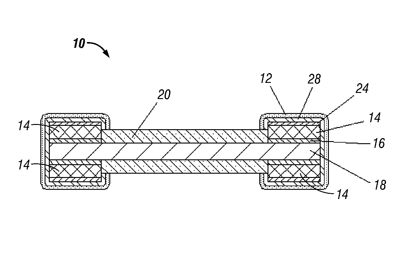
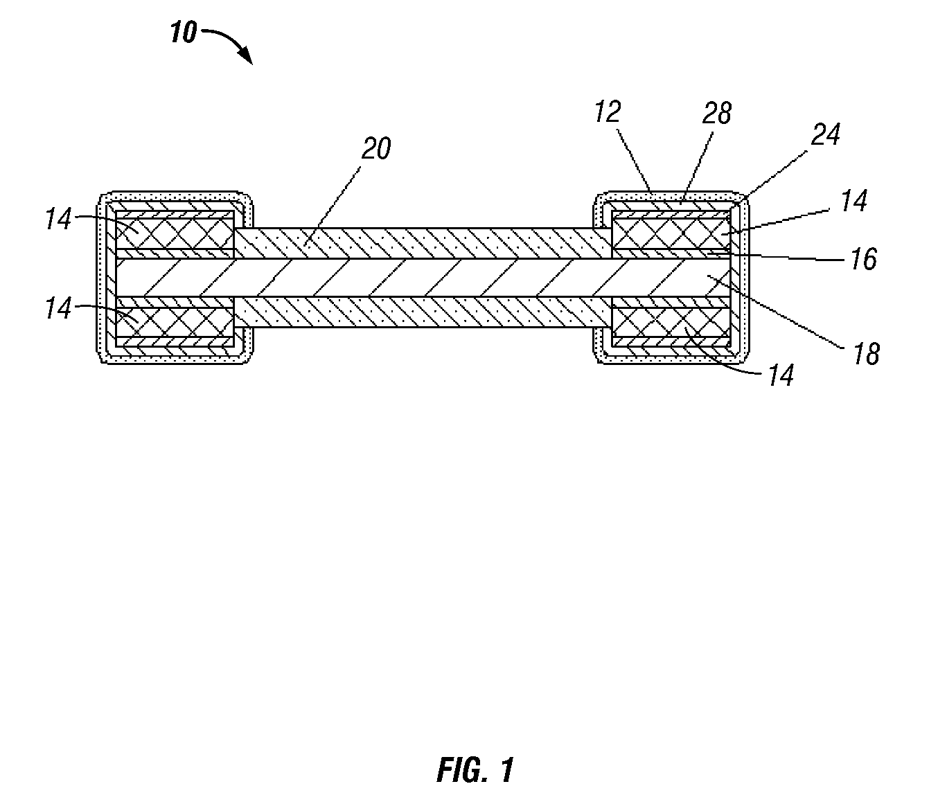
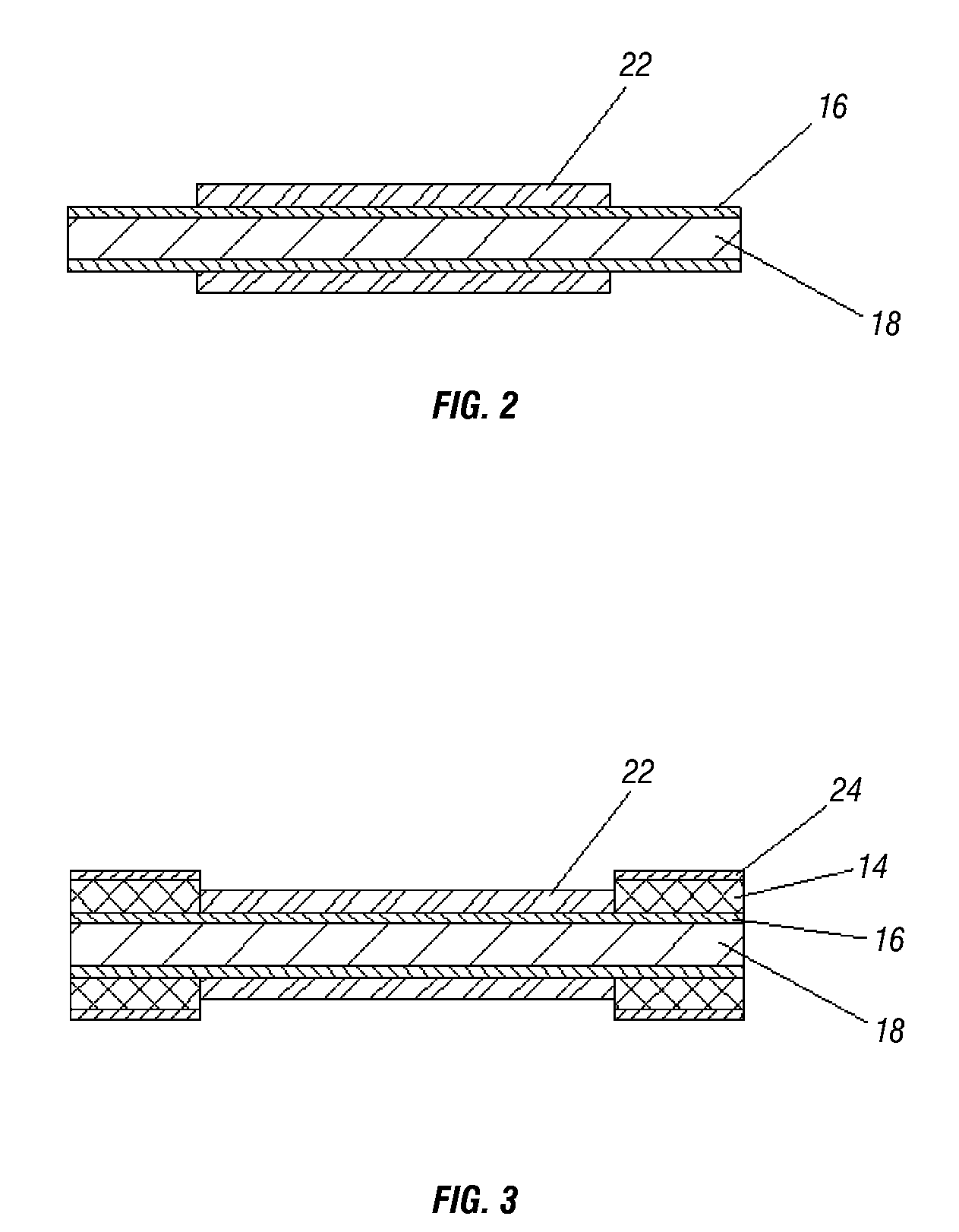
[0022]The present invention relates to metal strip resistor and a method of making metal strip resistors. The method is suitable for making an 0402 size or smaller, low ohmic value, metal strip surface mount resistor. An 0402 size is a standard electronics package size for certain passive components with 0.04 inch by 0.02 inch (1.0 mm by 0.5 mm) dimensions. One example of a smaller size of packaging which also may be used is an 0201 size. In the context of the present invention, a low ohmic value is generally a value suitable for applications in power-related applications. A low ohmic value is generally one that is less than or equal to 3 Ohms, but often times in the range of 1 to 1000 milliohms.

[0023]The method of manufacturing the metal strip resistor uses a process wherein the terminations of a resistor are formed by adding copper to the resistive material through sputtering and plating. This method utilizes photolithographic masking techniques that allow much smaller and better ...


PUM

PropertyMeasurementUnit
sizeaaaaaaaaaa
sizeaaaaaaaaaa
sizeaaaaaaaaaa

Abstract

A metal strip resistor is provided. The metal strip resistor includes a metal strip forming a resistive element and providing support for the metal strip resistor without use of a separate substrate. There are first and second opposite terminations overlaying the metal strip. There is plating on each of the first and second opposite terminations. There is also an insulating material overlaying the metal strip between the first and second opposite terminations. A method for forming a metal strip resistor wherein a metal strip provides support for the metal strip resistor without use of a separate substrate is provided. The method includes coating an insulative material to the metal strip, applying a lithographic process to form a conductive pattern overlaying the resistive material wherein the conductive pattern includes first and second opposite terminations, electroplating the conductive pattern, and adjusting resistance of the metal strip.

Description

BACKGROUND OF THE INVENTION[0001]The present invention relates to low resistance value metal strip resistors and a method of making the same.[0002]Metal strip resistors have previously been constructed in various ways. For example, U.S. Pat. No. 5,287,083 to Zandman and Person discloses plating nickel to the resistive material. However, such a process places limitations on the size of the resulting metal strip resistor. The nickel plating method is limited to large sizes because of the method for determining plating geometry. In addition, the nickel plating method has limitations on resistance measurement at laser trimming.[0003]Another approach has been to weld copper strips to the resistive material to form terminations. Such a method is disclosed in U.S. Pat. No. 5,604,477 to Rainer. The welding method is limited to larger size resistors because the weld dimensions take up space.[0004]Yet another approach has been to clad copper to the resistive material to form terminations such...

Claims


Application Information

Patent Timeline
Patent Type & Authority Patents(United States)
IPC IPC(8): H01C1/02
CPCH01C17/288H01C17/003H01C3/00H01C17/24H01C1/142Y10T29/49098Y10T29/49082
Inventor SMITH, CLARK L.BERTSCH, THOMAS L.WYATT, TODD L.VEIK, THOMAS L.BRUNE, RODNEY
Owner VISHAY DALE ELECTRONICS INC
Why Eureka
Try Eureka