Apparatus and method for investigating and/or modifying a sample

a technology of apparatus and sample, applied in the direction of tube electrostatic deflection, semiconductor/solid-state device testing/measurement, particle separator tube details, etc., can solve the problems of expensive and complicated disclosure solution, and achieve the effect of reducing the influence of charge accumulation effect and economics

Active Publication Date: 2012-08-21
CARL ZEISS SMT GMBH
View PDF41 Cites 9 Cited by
  • Summary
  • Abstract
  • Description
  • Claims
  • Application Information

AI Technical Summary

Benefits of technology

[0017]The objective lens advantageously comprises an electrostatic immersion lens by which the charged particles passing the lens are—in the direction of beam propagation of charged particles emitted by the charged particle source—decelerated from a higher kinetic energy in the range above 10 keV to a lower kinetic energy of 5 keV or less. By arranging the electrostatic deflection element on the low energy side of such immersion lens, i.e. on the side of the immersion lens on which the charged particles have the lower kinetic energy, the electrostatic deflection element can be operated with considerably lower voltages applied to its electrodes for deflecting the charged particle probe a predefined amount or angle. By this the advantage can be used that lower voltages can be applied and switched with considerably higher frequencies than higher voltages which makes it easier to reach high deflection bandwidths.
[0021]As a result, the preferred embodiment allows to omit conventionally used beam blanking elements and provides a more economic and a technically simpler solution. Furthermore a maintenance which requires venting of the electron-optical column and mechanical cleaning of a metal blade is no longer necessary, since the deflection and blanking element is attached underneath the actual column.
[0022]In the presently preferred embodiment, the apparatus further comprises a shielding element with an opening for the beam of charged particles to pass through, wherein the shielding element is arranged—in the direction of propagation of charged particles emitted by the charged particle source—downstream of the electrostatic deflection element. The distance d1 between the electrostatic deflection element and the shielding element is preferably in the range of 10 μm<d1<2.5 mm. The diameter of the opening of the shielding element and the distance d2 to the surface of a sample on which the charged particle probe is formed or the plane—perpendicular to the optical axis of the objective lens—in which the charged particle probe is formed by the objective lens, are preferably essentially the same. The shielding element is therefore sufficiently closely positioned to the surface in which the charge particle probe is formed to reduce the influence of charge accumulation effects at the surface of a sample arranged in that plane on the beam of charged particles.
[0028]Deflecting the beam by the three deflection systems, i.e. pre lens deflection system, lens, and post lens deflection system, now allows to scan a small image field at the sample (or in the plane in which the charged particle probe is formed). In addition, the post lens deflection system can deflect the beam so that it hits the rim of the aperture or the grid bar of a shielding mesh, so that the beam is effectively switched off or at least its intensity is reduced, without any essential changes of the spot position, where the (remaining) beam hits the surface of the sample.

Problems solved by technology

However, the disclosed solution is very complicated and costly.

Method used


Image

  • Apparatus and method for investigating and/or modifying a sample
  • Apparatus and method for investigating and/or modifying a sample
  • Apparatus and method for investigating and/or modifying a sample

Examples


Embodiment Construction

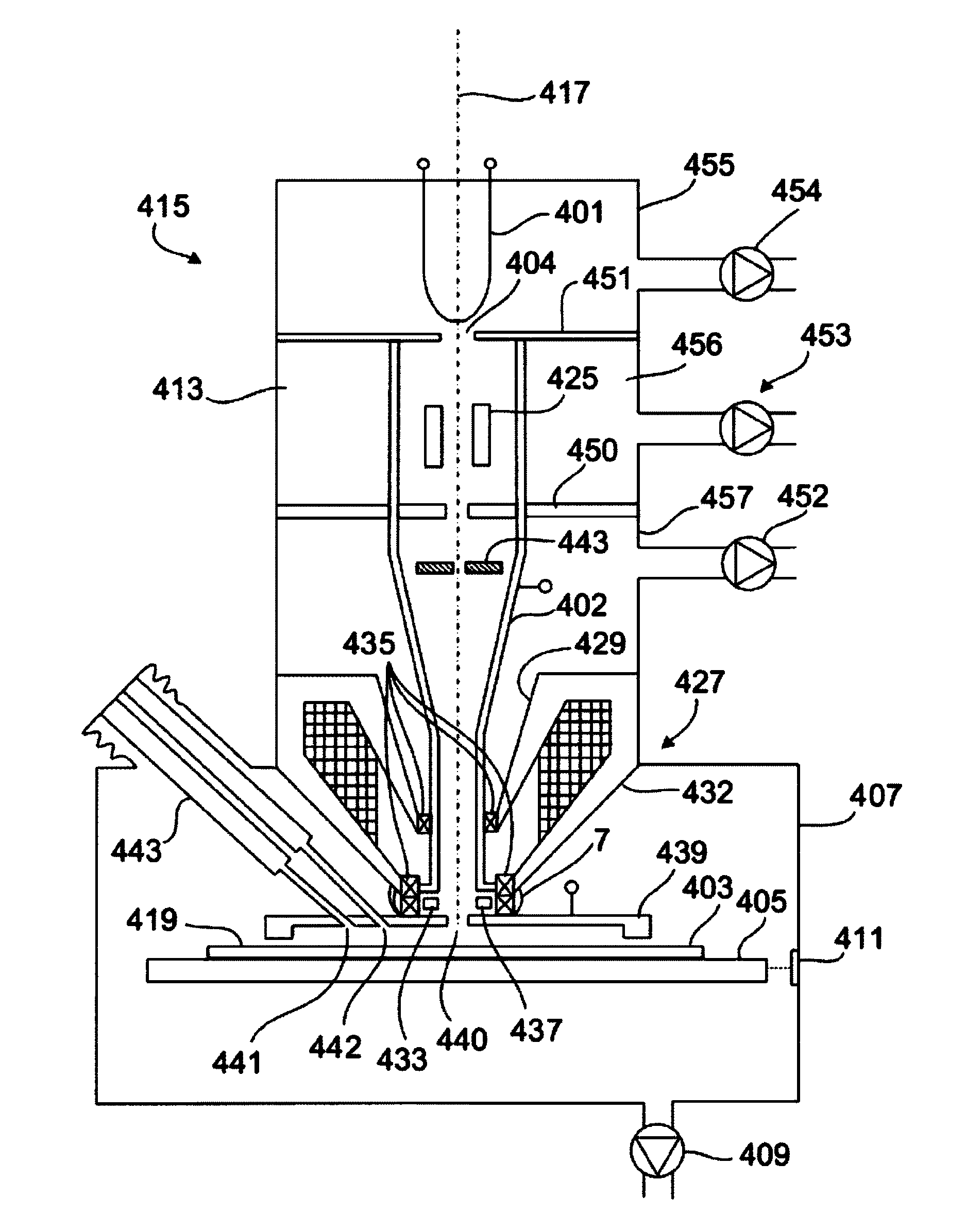
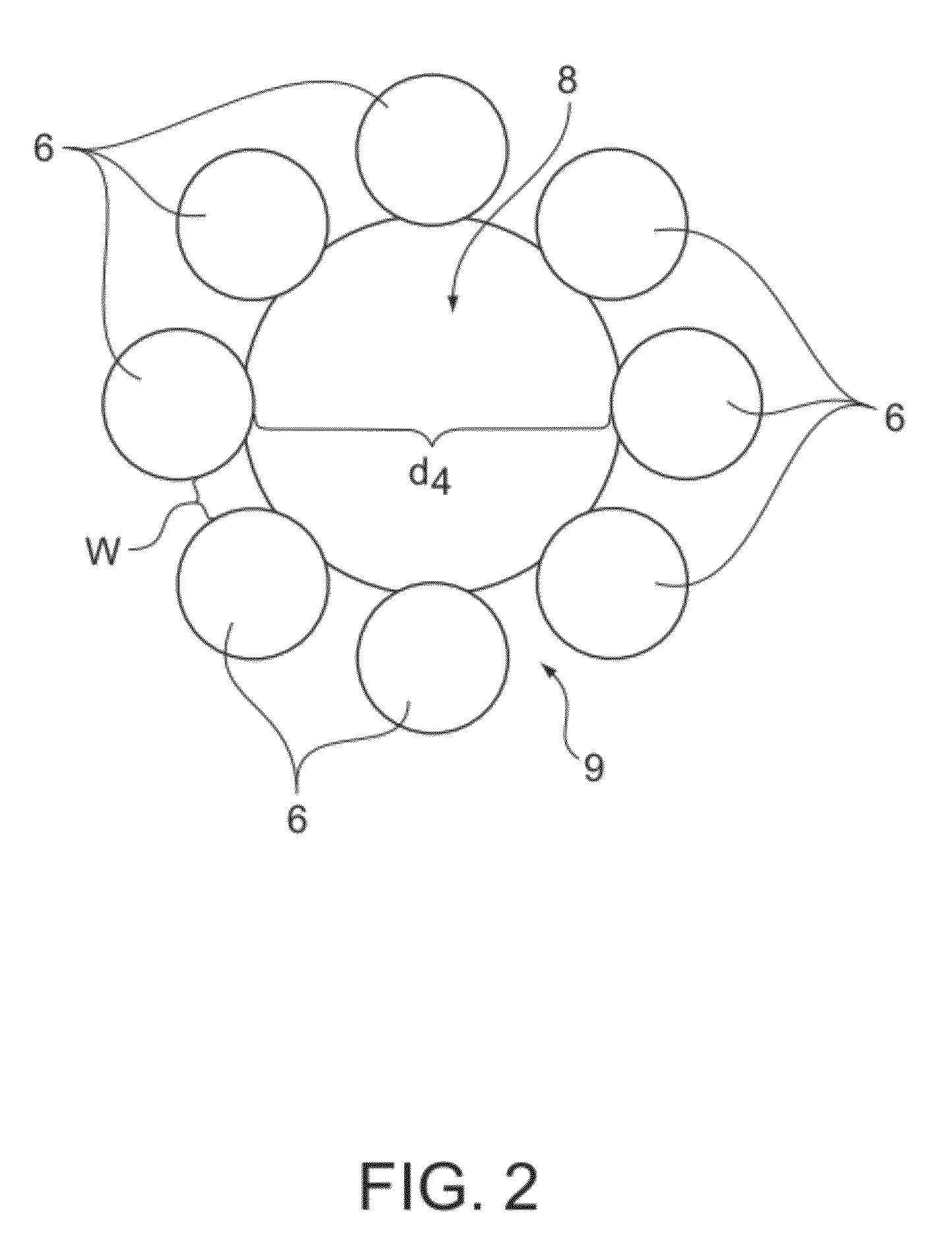
[0052]In the following, presently preferred embodiments of the claimed apparatus and the claimed method are described with particular reference to a scanning electron microscope. However, it is to be understood that the present invention can be used for any apparatus, wherein electrically charged particles are used to study, image or modify a sample either on its surface or in its interior regions. A particular important field of use is the repair of masks for the semiconductor industry. In this case the scanned electron beam is used to selectively deposit or remove material, in particular a chromium layer from the surface of the mask, which is typically made out of quartz.

[0053]FIG. 1 presents a schematic vertical cross-section of an embodiment of the invention. This system is used to process a work piece 403, namely a photo mask. This photo mask serves for use in a photolithographic process and carries structures which are photographically transferred to a radiation sensitive laye...


PUM

PropertyMeasurementUnit
kinetic end energyaaaaaaaaaa
timeaaaaaaaaaa
distanceaaaaaaaaaa

Abstract

An apparatus and a method for investigating and / or modifying a sample is disclosed. The apparatus comprises a charged particle source, at least one particle optical element forming a charged particle beam of charged particles emitted by said charged particle source. The apparatus further comprises an objective lens which generates a charged particle probe from said charged particle beam. The objective lens defines a particle optical axis. A first electrostatic deflection element is arranged—in a direction of propagation of charged particles emitted by said charged particle source—downstream of the objective lens. The electrostatic deflection element deflecting the charged particle beam in a direction perpendicular to said charged particle optical axis and has a deflection bandwidth of at least 10 MHz.

Description

CROSS-REFERENCE TO RELATED APPLICATIONS[0001]This application is a continuation of, and claims benefit under 35 USC 120 to, international application PCT / EP2008 / 068220, filed Dec. 23, 2008, which claims the benefit of U.S. Provisional Application Ser. No. 61 / 016,724, filed Dec. 26, 2007. International application PCT / EP2008 / 068220 is hereby incorporated by reference in its entirety.1. TECHNICAL FIELD[0002]The present invention relates to an apparatus and a method for investigating and / or modifying a sample with a beam of charged particles, in particular a beam of electrons.2. THE PRIOR ART[0003]In many microscopy techniques such as scanning electron or scanning ion microscopy, a focused beam of charged particles is scanned across the sample. The particles, which are emitted or scattered from the sample, are collected by a detector to provide a two-dimensional image. Scanned beams of electrons are also used for modifying the surface, for example by selectively removing or depositing ...

Claims


Application Information

Patent Timeline
Patent Type & Authority Patents(United States)
IPC IPC(8): H01J49/22G21K5/02
CPCC23F4/00H01J37/3056H01L21/76894H01L22/22H01J2237/28H01J2237/3174H01L2924/0002H01L2924/00
Inventor EDINGER, KLAUSBECKER, RAINERBUDACH, MICHAELHOFMANN, THORSTEN
Owner CARL ZEISS SMT GMBH
Why Eureka
Try Eureka