Organic electroluminescent display device and method of fabricating the same
a technology of electroluminescent display and organic eld, which is applied in the direction of discharge tube luminescnet screen, discharge tube/lamp details, electric discharge lamps, etc., can solve the problems of limited display size relatively high operating power of passive matrix organic eld device, so as to improve the display quality and ensure the effect of conta
- Summary
- Abstract
- Description
- Claims
- Application Information
AI Technical Summary
Benefits of technology
Problems solved by technology
Method used
Image
Examples
first embodiment
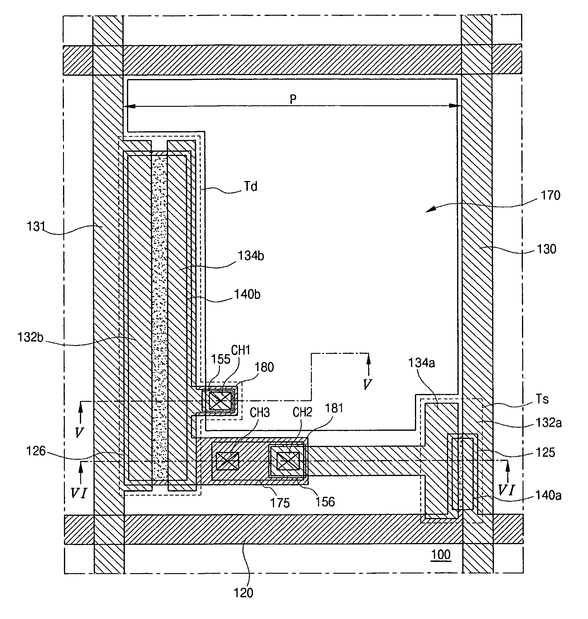
[0032]FIG. 4 is a plane view showing an array substrate for an organic electroluminescent display device according to the present invention.
[0033]In FIG. 4, a gate line 120, a data line 130 and a power line 131 are formed on a substrate 100. The gate line 120 crosses the data line 130 to define a pixel region P, and the power line 130 is parallel to and spaced apart from the data line 130. The substrate 100 includes a transparent material such as glass and plastic. A switching element Ts is connected to the gate line 120 and the data line 130, and a driving element Td is connected to the switching element Ts. The switching element Ts includes a first gate electrode 125, a first active layer 140a, a first ohmic contact layer (not shown), a first source electrode 132a and a first drain electrode 134a. In addition, the driving element Td includes a second gate electrode 126, a second active layer 140b, a second ohmic contact layer (not shown), a second source electrode 132b and a secon...
second embodiment
[0048]FIG. 7 is a plane view showing an array substrate for an organic electroluminescent display device according to the present invention.
[0049]In FIG. 7, a gate line 220, a data line 230 and a power line 231 are formed on a substrate 200. The gate line 220 crosses the data line 230 to define a pixel region P, and the power line 230 is parallel to and spaced apart from the data line 230. The substrate 200 includes a transparent material such as glass and plastic. A switching element Ts is connected to the gate line 220 and the data line 230, and a driving element Td is connected to the switching element Ts. The switching element Ts includes a first gate electrode 225, a first active layer 240a, a first ohmic contact layer (not shown), a first source electrode 232a and a first drain electrode 234a. In addition, the driving element Td includes a second gate electrode 226, a second active layer 240b, a second ohmic contact layer (not shown), a second source electrode 232b and a secon...
third embodiment
[0069]FIG. 10 is a plane view showing an array substrate for an organic electroluminescent display device according to the present invention.
[0070]In FIG. 10, a gate line 320, a data line 330 and a power line 331 are formed on a substrate 300. The gate line 320 crosses the data line 330 to define a pixel region P, and the power line 330 is parallel to and spaced apart from the data line 330. The substrate 300 includes a transparent material such as glass and plastic. A switching element Ts is connected to the gate line 320 and the data line 330, and a driving element Td is connected to the switching element Ts. The switching element Ts includes a first gate electrode 325, a first active layer 340a, a first ohmic contact layer (not shown), a first source electrode 332a and a first drain electrode 334a. In addition, the driving element Td includes a second gate electrode 326, a second active layer 340b, a second ohmic contact layer (not shown), a second source electrode 332b and a sec...
PUM
 Abstract
Description
Claims
Application Information


