Method of constructing a differential inductor

a technology of differential inductors and inductors, which is applied in the field of improved design of differential inductors, can solve the problems of consuming more space, consuming more space, and inherently difficult to miniaturize components, and achieves the effects of reducing the effective capacitance of differential inductors, and increasing self-resonance frequency

Active Publication Date: 2012-10-02
QORVO US INC
View PDF22 Cites 10 Cited by
  • Summary
  • Abstract
  • Description
  • Claims
  • Application Information

AI Technical Summary

Benefits of technology

[0009]The present invention winds the coils of a differential inductor to provide partial electrical shielding between the two branches by staggering the branches with respect to one another. The staggering causes the portions of the loops of the coil with the most voltage swing thereon to be positioned proximate portions that are close to ground and thus have little or no voltage swing. This positioning lowers the effective capacitance of the differential inductor and allows for a higher self-resonance frequency. This in turn allows for a broader range of operating frequencies. In effect, the present invention shields those portions of the differential inductor that are highly positive or highly negative from one another by positioning portions of the differential inductor that are close to ground therebetween.
[0010]The mitigation of the effective capacitance is accomplished with little or no sacrifice in magnetic coupling. In this regard, this invention is based on the fact that effective capacitance is dependent on charge and voltage swings of electrically coupled elements, while mutual inductance is dependent on electric current through magnetically coupled elements. The mutual inductance is desirable when the current winds in the same sense (e.g., clockwise or counterclockwise) under the differential driving condition. This invention tends to conserve the totality of desirable couplings of current segments relative to the conventional implementations, while reducing the capacitive coupling of the oppositely driven branches of the differential inductor. Only the totality of the desirable magnetic couplings of current carrying segments is important to the total effective inductance of a branch, and not the segments' identification with one branch or the other. Thus, as the structure is staggered to minimize the effective capacitance, the magnetic coupling in totality is preserved, because for every segment that is moved away for effective capacitance reasons, another segment takes its place with the same spacing and sense of current direction, effectively preserving the total inductance.

Problems solved by technology

Some components are inherently difficult to miniaturize.
First, spreading the loops consumes more space, which, as already mentioned, is at a premium in mobile terminals.
This lower inductance is offset by adding windings, which also takes up more space.

Method used


Image

  • Method of constructing a differential inductor
  • Method of constructing a differential inductor
  • Method of constructing a differential inductor

Examples


Embodiment Construction

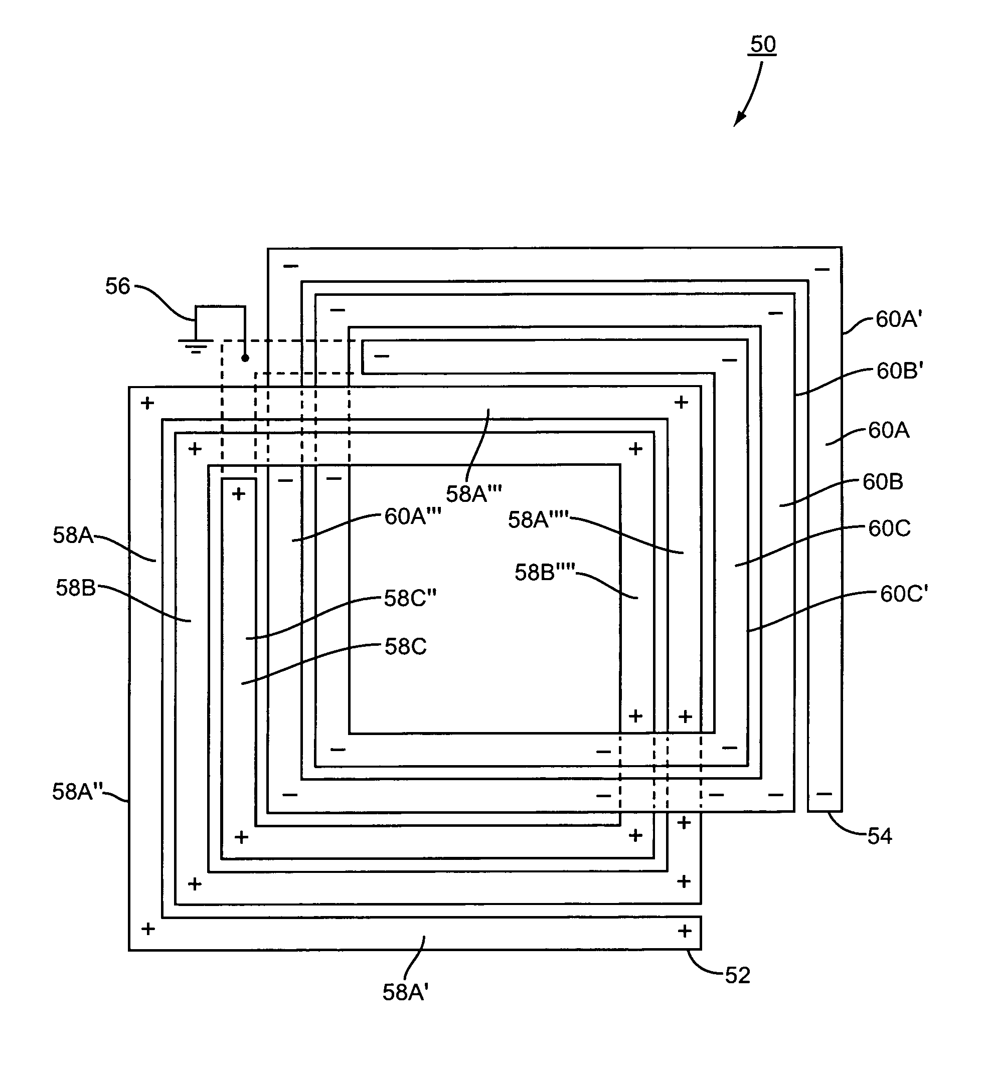
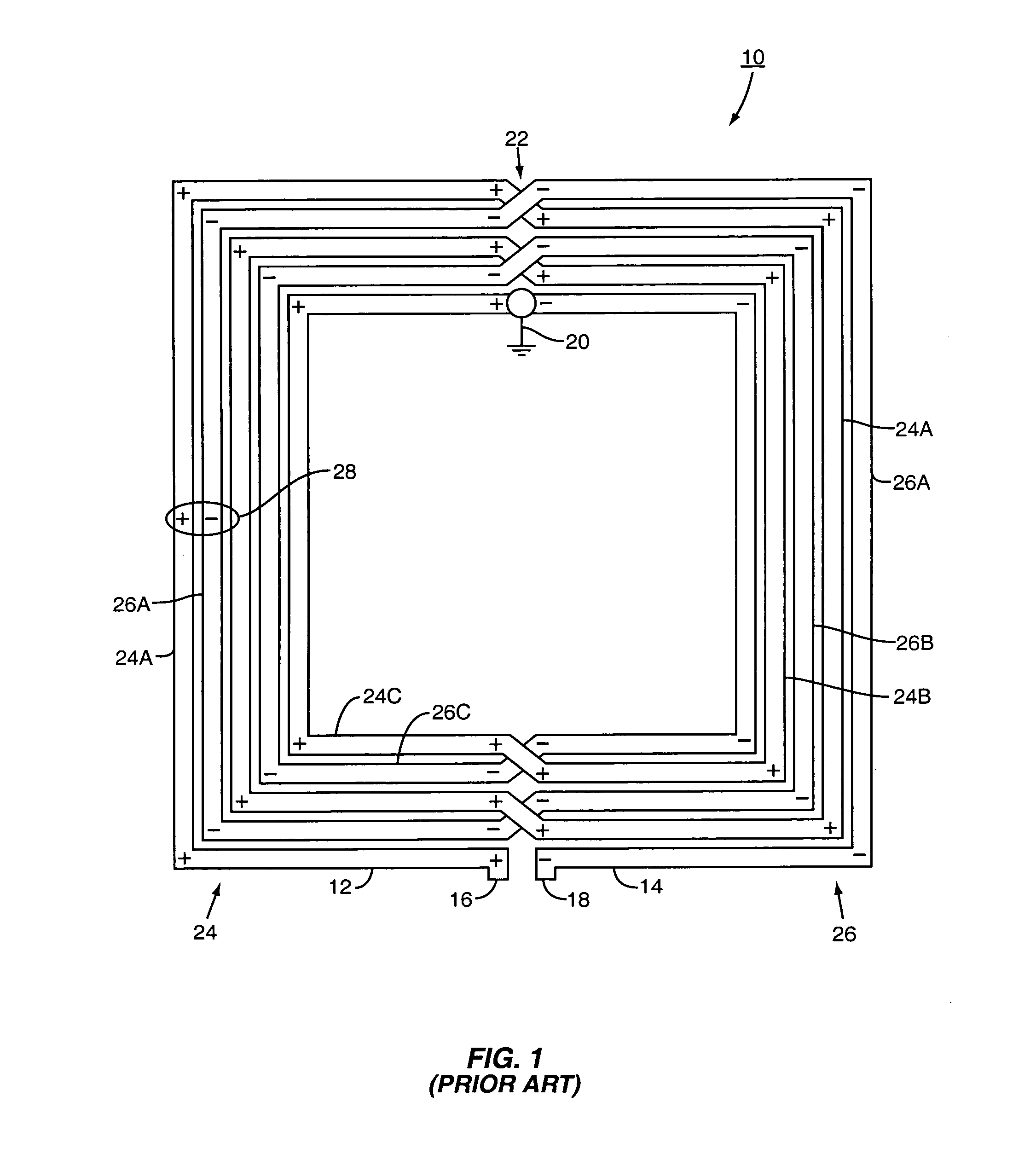
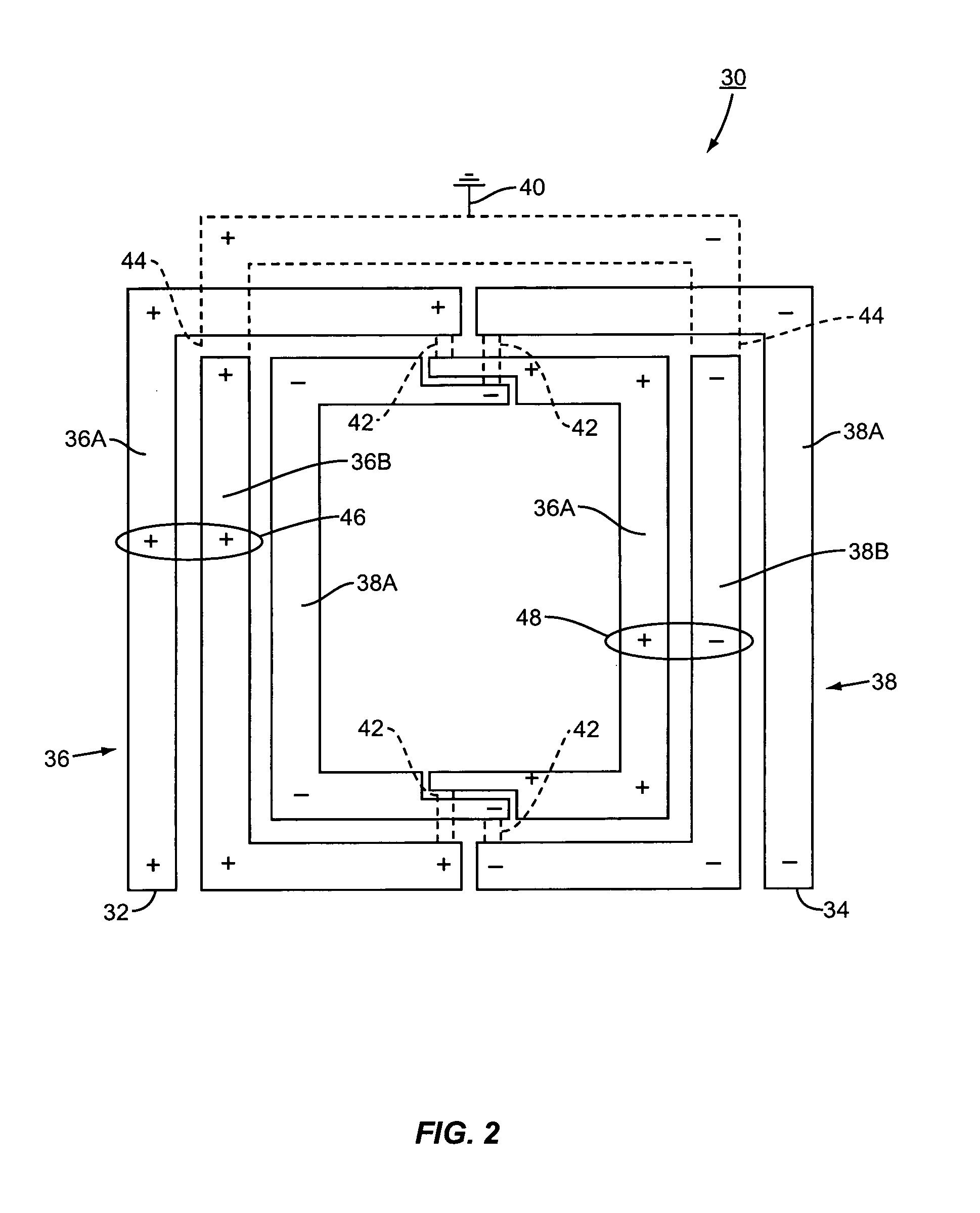
[0021]The embodiments set forth below represent the necessary information to enable those skilled in the art to practice the invention and illustrate the best mode of practicing the invention. Upon reading the following description in light of the accompanying drawing figures, those skilled in the art will understand the concepts of the invention and will recognize applications of these concepts not particularly addressed herein. It should be understood that these concepts and applications fall within the scope of the disclosure and the accompanying claims.

[0022]The present invention is an improved differential inductor suitable for use in an on-chip voltage controlled oscillator (VCO), a tuned amplifier, a power amplifier, an up-conversion mixer or similar electronic component that uses a differential inductor and for which there are demands to conserve space. However, the present invention is not limited to such environments and can be used in any environment in which an inductor ...


PUM

PropertyMeasurementUnit
inductanceaaaaaaaaaa
electricallyaaaaaaaaaa

Abstract

A method of constructing a differential inductor having a high self-resonance frequency is provided. In general, a ground point is identified. A first coil having a first and second loop is created such that the first loop is electrically further away from the ground point than the second loop. A second coil having a third and fourth loop are created such that the third loop is electrically further away from the ground point than the second loop. The first coil and the second coil are positioned such that the first loop is positioned as a near neighbor to said fourth loop and said second loop is positioned as a near neighbor to said third loop.

Description

[0001]This application is a Divisional of application Ser. No. 10 / 704,869, filed Nov. 10, 2003, now U.S. Pat. No. 6,972,658 B1, the disclosure of which is incorporated herein by reference in its entirety.FIELD OF THE INVENTION[0002]The present invention is directed to an improved design for differential inductors that has a high self-resonance frequency.BACKGROUND OF THE INVENTION[0003]As of this writing, wireless devices have become ubiquitous in American society. Pagers, cellular telephones, personal digital assistants and the like (collectively “mobile terminals”) can be found in home and business environments. Likewise, the availability of affordable wireless routers has caused a surge in the number of wireless local area networks. Common to most of these devices are wireless transmitters and receivers. In these wireless transmitters and receivers, it is common to have an on-chip voltage controlled oscillator (VCO), a tuned amplifier, a power amplifier, or an up-conversion mixer...

Claims


Application Information

Patent Timeline
Patent Type & Authority Patents(United States)
IPC IPC(8): H01F7/06H01F5/00H01F17/00H01L23/522
CPCH01F17/0006H01L23/5227H01F17/0013H01F2017/0046H01F2021/125Y10T29/49064Y10T29/49073Y10T29/49071Y10T29/49194H01L2924/0002
Inventor FINDLEY, PAULTAO, JONREZVANI, GHOLAM-ALI
Owner QORVO US INC
Why Eureka
Try Eureka