Method for producing a multilayer piezoelectric microcomponent using sacrificial thick film technology

a piezoelectric microcomponent and film technology, applied in the direction of piezoelectric/electrostrictive transducers, resistive material coatings, transducer types, etc., can solve the problems of inability to manufacture components in a collective manner, time-consuming and costly methods, and inability to manufacture components in a single atmosphere, etc., to achieve the effect of reliable and relatively simple obtaining

Inactive Publication Date: 2012-10-16
CENT NAT DE LA RECHERCHE SCI
View PDF22 Cites 3 Cited by
  • Summary
  • Abstract
  • Description
  • Claims
  • Application Information

AI Technical Summary

Problems solved by technology

However, these methods are time-consuming and costly, because they comprise numerous micromachining steps (masking, etching, deposition, etc.).
However, these techniques are not suitable for the collective manufacture of components.
Moreover, this atmosphere may be prohibitive for the manufacture of numerous materials that are unstable under this atmosphere.

Method used


Image

  • Method for producing a multilayer piezoelectric microcomponent using sacrificial thick film technology
  • Method for producing a multilayer piezoelectric microcomponent using sacrificial thick film technology
  • Method for producing a multilayer piezoelectric microcomponent using sacrificial thick film technology

Examples


example 1

Thermal Actuator

Preparation of a Thermal Actuator

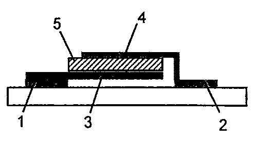
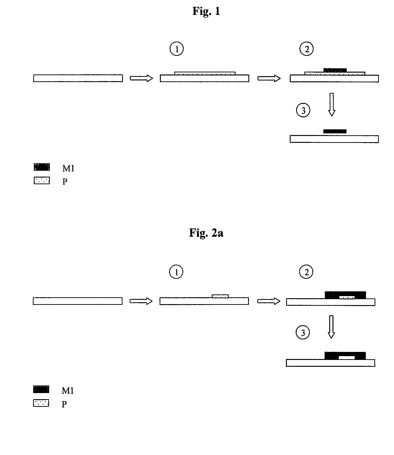
[0193]A thermal actuator shown in FIG. 10 was prepared by the method of the invention, on an alumina substrate.

[0194]The dimensions of the arms 1 and 2 are as follows:

[0195]

ArmLengthThicknessWidth13.3 mm22 μm590 μm22.4 mm22 μm140 μm

[0196]FIG. 12a shows the various steps of the method in a plan view.

[0197]FIG. 12b show the steps of the method in a side view along line A-A shown in FIG. 12a. [0198]A film of material P is deposited on a substrate during the step {circle around (1)}, and said film is consolidated;[0199]during step {circle around (2)}, a film of material M1 is deposited, alongside the film P, in the form of two zones corresponding to the pads under the zone 3 and 4 of the actuator, and said film M1 is partially consolidated;[0200]during the step {circle around (3)}, a film of material M′1 is deposited according to the pattern shown in FIGS. 12a and 12b, and a total consolidation is carried out;[0201]during step {circle aro...

example 2

Heating Resistors

Preparation of the Heating Resistor

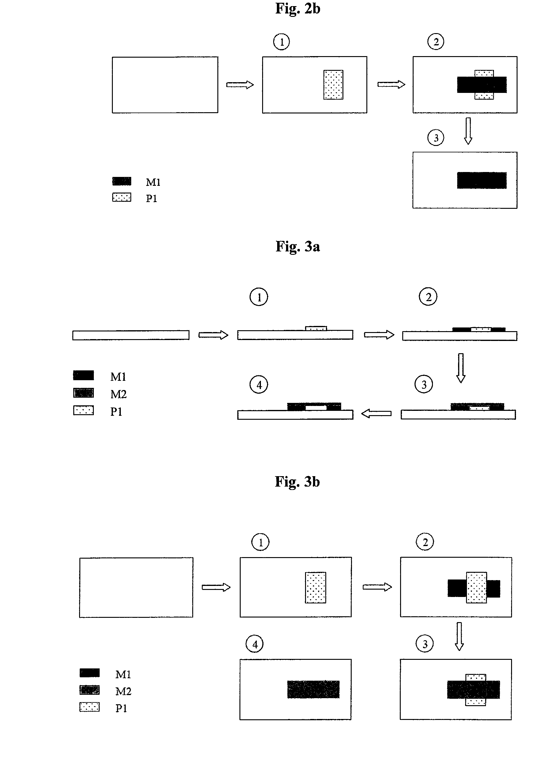
[0212]A resistor as shown in FIG. 13a was prepared.

[0213]FIG. 13a shows the various steps of a method in a plan view.

[0214]FIG. 13b show the steps of the method in a side view along line A-A shown in FIG. 11a. [0215]On a substrate, during the step {circle around (1)}, a film of material P is deposited, and said film is consolidated in the conditions indicated in example 1;[0216]during step {circle around (2)}, a film of material M1 is deposited, alongside the film P and along the same side of the film P, in the form of two zones corresponding to the pads under the zones 11 and 12 of the resistor (FIG. 11a), and said film M1 is partially consolidated in the conditions indicated in test 2 of example 1;[0217]during step {circle around (3)}, a film of ink M′1 is deposited according to the pattern shown in FIG. 13a and representing the shape of the filament, and a partial consolidation is carried out in the conditions indicated for test...

example 3

Preparation of Microchannels

[0230]Microchannels were prepared by the process shown schematically in FIGS. 14a and 14b. FIG. 14a shows a plan view, and FIG. 14b shows a side view along line A-A indicated in step {circle around (3)} of FIG. 14a. [0231]An ink P is deposited on a substrate during step {circle around (1)}, and said film is consolidated in the same conditions as in example 1;[0232]during step {circle around (2)}, along two opposite edges of the film of ink P, a film of ink M1 is deposited, in the form of two zones corresponding to the side walls of the desired microchannel, and said film of ink M1 is partially consolidated;[0233]during step {circle around (3)}, a film of ink P forming the upper wall of the microchannel is deposited above the film P and the film M1, an ink film M′1 forming the upper wall of the microchannel, and a total consolidation is carried out;[0234]during step {circle around (4)}, the material P is removed in the conditions indicated in example 1.

[02...


PUM

PropertyMeasurementUnit
temperatureaaaaaaaaaa

Abstract

The invention relates to the preparation of multilayer microcomponents which comprise one or more films, each consisting of a material M selected from metals, metal alloys, glasses, ceramics and glass-ceramics.The method consists in depositing on a substrate one or more films of an ink P, and one or more films of an ink M, each film being deposited in a predefined pattern selected according to the structure of the microcomponent, each film of ink P and each film of ink M being at least partially consolidated before deposition of the next film; effecting a total consolidation of the films of ink M partially consolidated after their deposition, to convert them to films of material M; totally or partially removing the material of each of the films of ink P. An ink P consists of a thermoset resin containing a mineral filler or a mixture comprising a mineral filler and an organic binder. An ink M consists of a mineral material precursor of the material M and an organic binder. The inks are deposited by pouring or by extrusion.

Description

[0001]The present invention relates to the preparation of multilayer microcomponents which may constitute a microsystem or part of a millimeter-sized microsystem, said microcomponents being at least partially released from the substrate on which they are prepared by the sacrificial thick film method.BACKGROUND OF THE INVENTION[0002]Numerous components having micron- or millimeter-sized dimensions are used for the preparation of various Microsystems, particularly in the fields of microelectronics, microrobotics, micromechanics, microfluidics, micromagnetism, microthermics, microoptics, or microchemistry. The various economic sectors concerned are in particular those of the automobile, space, aeronautics, home automation, health, biology, chemistry, agrifood industry, and the environment. These components may have a wide variety of shapes and they may consist of varied materials, according to their intended use. They are used in Microsystems generally designated as MEMS (MicroElectro-...

Claims


Application Information

Patent Timeline
Patent Type & Authority Patents(United States)
IPC IPC(8): B05D5/12H01L41/22H01L21/00B32B3/00H01L41/00B81C99/00H01L41/29H01L41/39
CPCB81C99/0095H01L41/29H01L41/27H01L41/314B81B2201/0271B81B2201/031B81B2203/0109B81B2203/0118Y10T428/24926Y10T29/42Y10T428/24917H01L41/107H10N30/40H10N30/05H10N30/06H10N30/074
Inventor LUCAT, CLAUDEMENIL, FRANCISDEBEDA-HICKEL, HELENEGINET, PATRICK
Owner CENT NAT DE LA RECHERCHE SCI
Why Eureka
Try Eureka