

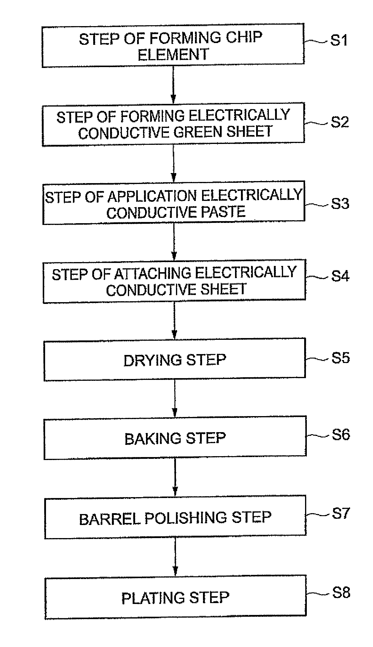
Method for manufacturing electronic component
a technology of electronic components and manufacturing methods, applied in the direction of fixed capacitor details, semiconductor/solid-state device details, fixed capacitors, etc., can solve the problems of decreasing the reliability of electronic components, and achieve the effect of increasing the content ratio of electrically conductive materials, increasing the electric conductivity of external electrodes, and convenient shaping
- Summary
- Abstract
- Description
- Claims
- Application Information
AI Technical Summary
Benefits of technology
Problems solved by technology
Method used
Image

Examples
embodiment 1
[0048
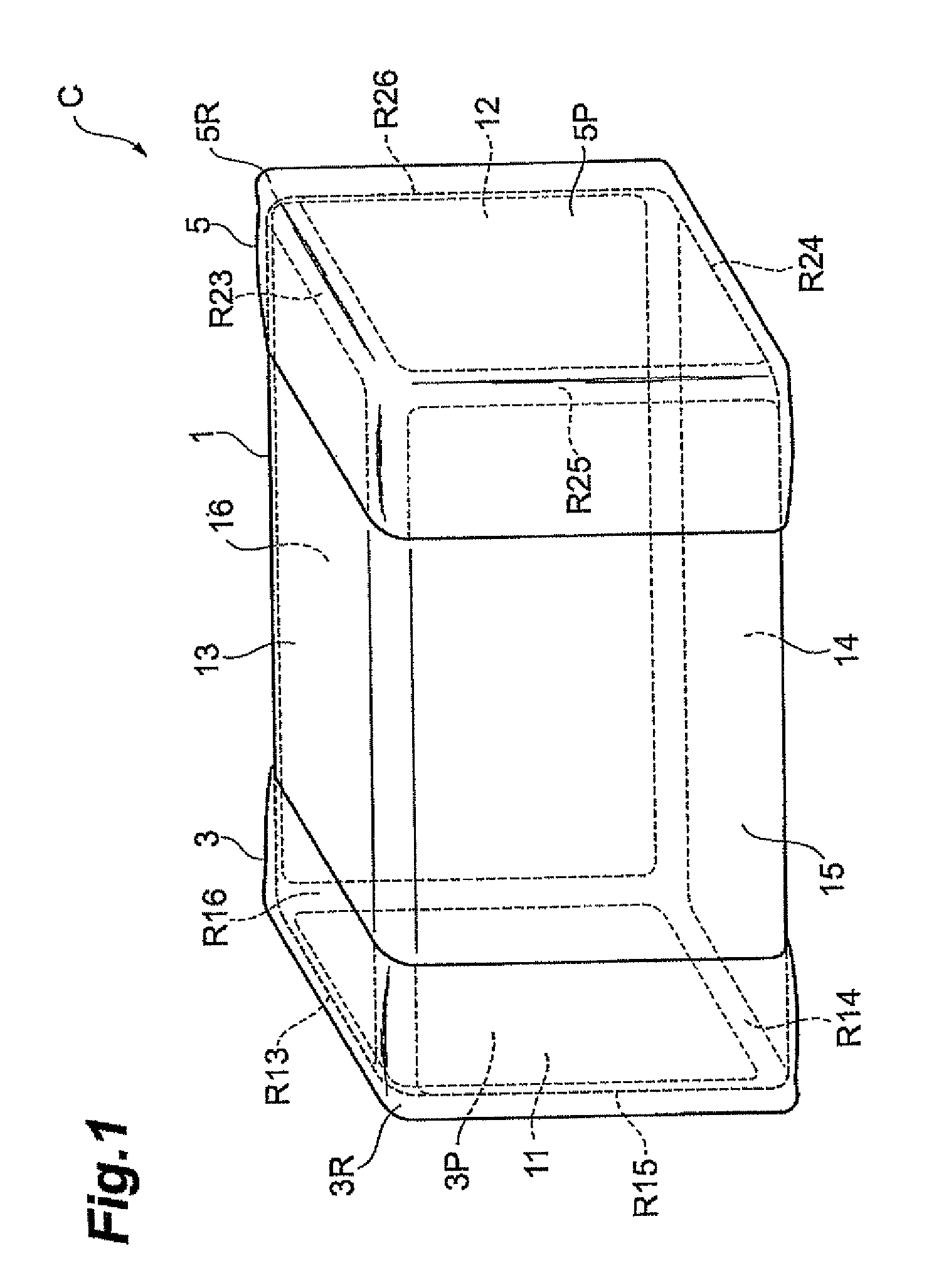
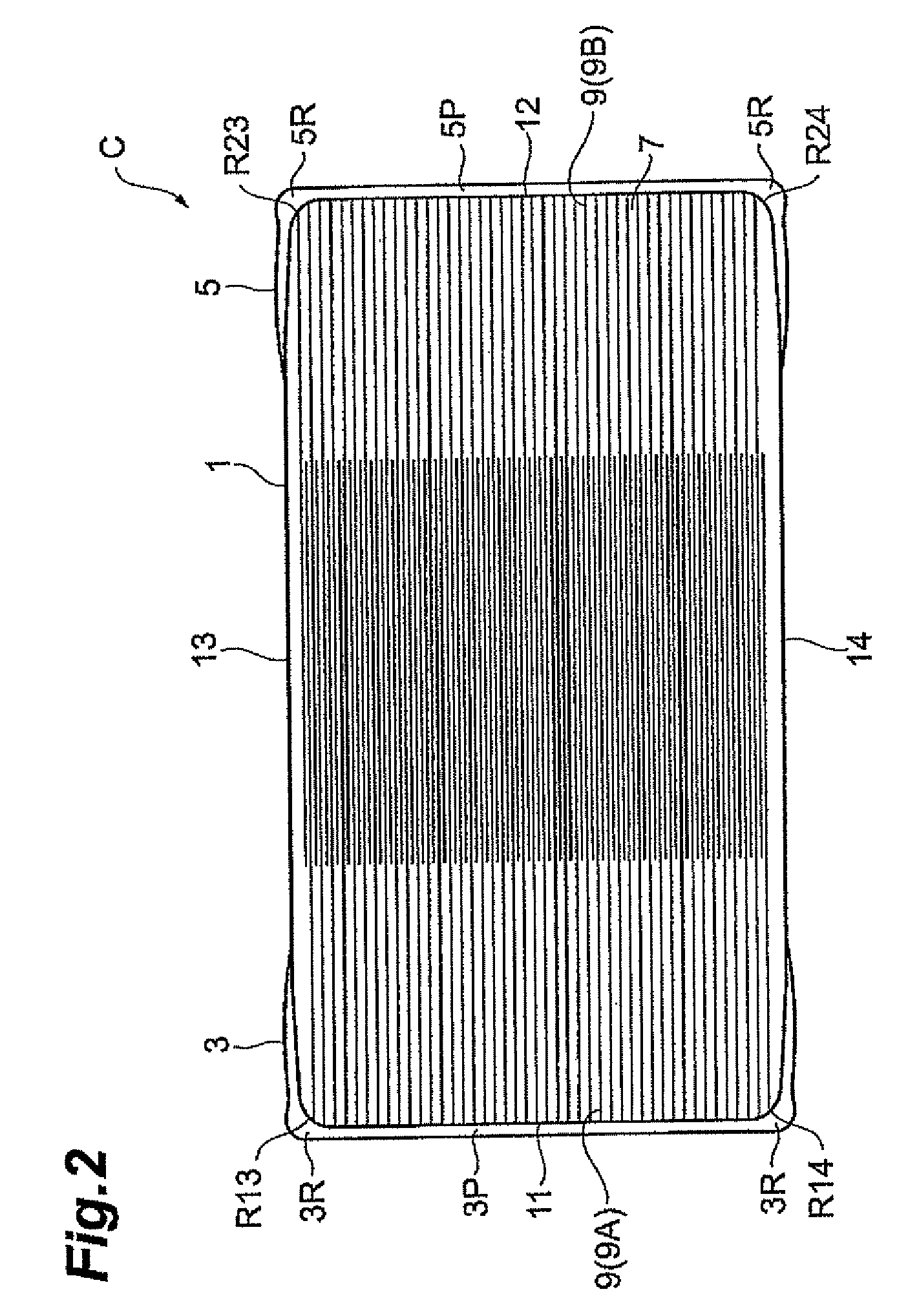
[0049]First an electronic component C of the present embodiment will be explained with reference to FIG. 1 and FIG. 2. FIG. 1 is a perspective view of the electronic component of the present embodiment FIG. 2 is a cross-sectional view of the electronic component of the present embodiment. The electronic component C of the present embodiment is a chip-like multilayer ceramic capacitor. The electronic component C is in the form of a substantially rectangular parallelepiped and, for example, has a length in the longitudinal (transverse) direction of about 1.0 mm and a length in the width direction and a length in the depth direction of about 0.5 mm.
[0050]The electronic component C includes a chip element 1 in the form of a substantially rectangular parallelepiped, and a first external electrode 3 and a second external electrode 5 formed on respective end portions of the chip element 1. The chip element 1 has mutually opposing end surface 11 and end surface 12, mutually opposing si...
embodiment 2
[0094
[0095]An electronic component C100 of Embodiment 2 will be explained below with reference to FIG. 11 and FIG. 12. FIG. 11 is a perspective view of the electronic component of the present embodiment. FIG. 12 is a cross-sectional view of the electronic component of the present embodiment. The electronic component C100 of the present embodiment is a chip-like multilayer ceramic capacitor. The electronic component C100 is in the form of a substantially rectangular parallelepiped and, for example, has a let in the longitudinal (transverse) direction of about 1.0 mm and a length in the width direction and a length in the depth direction of about 0.5 mm
[0096]The electronic component C100 includes a chip element 101 in the form of a substantially rectangular parallelepiped, and a first external electrode 103 and a second external electrode 105 formed on respective end portions of the chip element 101. The chip element 101 has mutually opposing end surface 111 and end surface 112, mutua...
PUM
| Property | Measurement | Unit |
|---|---|---|
| length | aaaaa | aaaaa |
| length | aaaaa | aaaaa |
| thickness | aaaaa | aaaaa |
Abstract
Description
Claims
Application Information