Display device, method for driving same, and electronic apparatus

a display device and display method technology, applied in the direction of instruments, computing, electric discharge tubes, etc., can solve the problems of increasing the degree of complexity and the scale of the vertical drive circuit, the pixel array part, and the increase in the number of stages so as to reduce the scale of the peripheral vertical drive circuit, reduce the scale of the shift register, and reduce the scale of the circuit scale

Active Publication Date: 2012-10-23
JOLED INC
View PDF17 Cites 3 Cited by
  • Summary
  • Abstract
  • Description
  • Claims
  • Application Information

AI Technical Summary

Benefits of technology

[0007]The related-art display devices have a configuration in which a pixel array part and a drive part are integrally formed over one panel. The pixel array part at the center of the panel is formed of an aggregation of pixels arranged in a matrix. The drive part is disposed in the peripheral frame area surrounding the center pixel array part, and drives the pixel array part disposed in the center area from the periphery. The pixel array part includes row first drive lines disposed corresponding to the rows of the pixels, row second drive lines disposed corresponding to the rows of the pixels similarly, and column signal lines disposed corresponding to the columns of the pixels. In matching with this configuration, the drive part includes a horizontal drive circuit that supplies a video signal to the column signal lines, and a first vertical drive circuit and a second vertical drive circuit that cause the light-emission operation of the pixels on a row-by-row basis via the row first drive lines and the row second drive lines, respectively. Based on this configuration, the drive part allows displaying of the image dependent upon the video signal on the pixel array part.
[0010]If the number of rows of the pixels (the number of lines) is increased along with enhancement in the definition and the density of the pixel array part, the number of drive lines for driving the pixels on a row-by-row basis is also correspondingly increased. In linkage with the increase in the density of the drive lines, the size of the interconnect pattern thereof needs to be decreased and the distance between adjacent interconnect patterns also needs to be decreased. This results in a problem that short-circuit defects in the pixel array part frequently occur and therefore the yield is lowered.
[0012]According to the embodiment of the present invention, the first vertical drive circuit simultaneously drives the pixels on two rows adjacent to each other. In other words, each stage of the shift registers included in the first vertical drive circuit corresponds to the pixels on two rows (two lines), and thus the scale of the shift registers can be halved. Similarly, the second vertical drive circuit also simultaneously drives the pixels on two rows adjacent to each other, which allows reduction in the circuit scale thereof. The pair of pixel rows simultaneously driven by the first vertical drive circuit and the pair of pixel rows simultaneously driven by the second vertical drive circuit are shifted from each other by one row (i.e. are so set as to be in a staggered relationship). This allows the light-emission operation of the pixels on a row-by-row basis. That is, it is possible to sequentially-drive the pixel rows while reducing the scale of the peripheral vertical drive circuitry. By thus simplifying the peripheral vertical drive circuitry, the frame size of the panel can be decreased and an effect of reduction in the power consumption can also be achieved.
[0013]By employing the operation sequence in which the pixels on two rows adjacent to each other are simultaneously driven, the drive line can be shared by the pixels on two rows adjacent to each other depending on the pixel layout. That is, the number of drive lines can be halved compared with the related arts. This allows achievement of enhancement in the definition of the pixel array part, increase in the pixel capacitance, and reduction in short-circuit defects between interconnects.

Problems solved by technology

Increase in the number of rows of the pixels inevitably leads to increase in the number of stages of the shift registers.
This causes increases in the degree of complexity and the scale of the vertical drive circuit, which is a problem that should be solved.
This results in a problem that short-circuit defects in the pixel array part frequently occur and therefore the yield is lowered.

Method used


Image

  • Display device, method for driving same, and electronic apparatus
  • Display device, method for driving same, and electronic apparatus
  • Display device, method for driving same, and electronic apparatus

Examples


Embodiment Construction

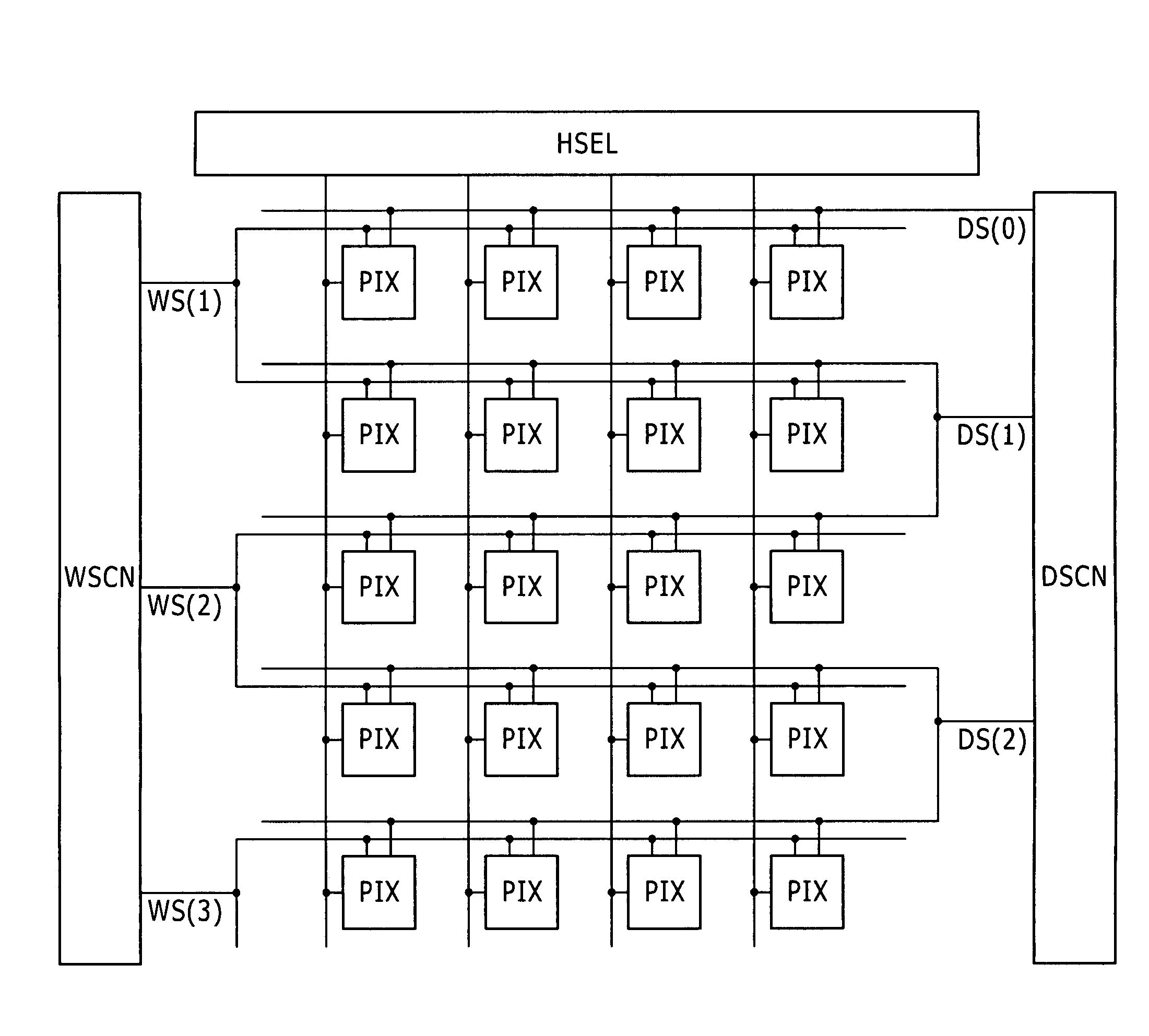
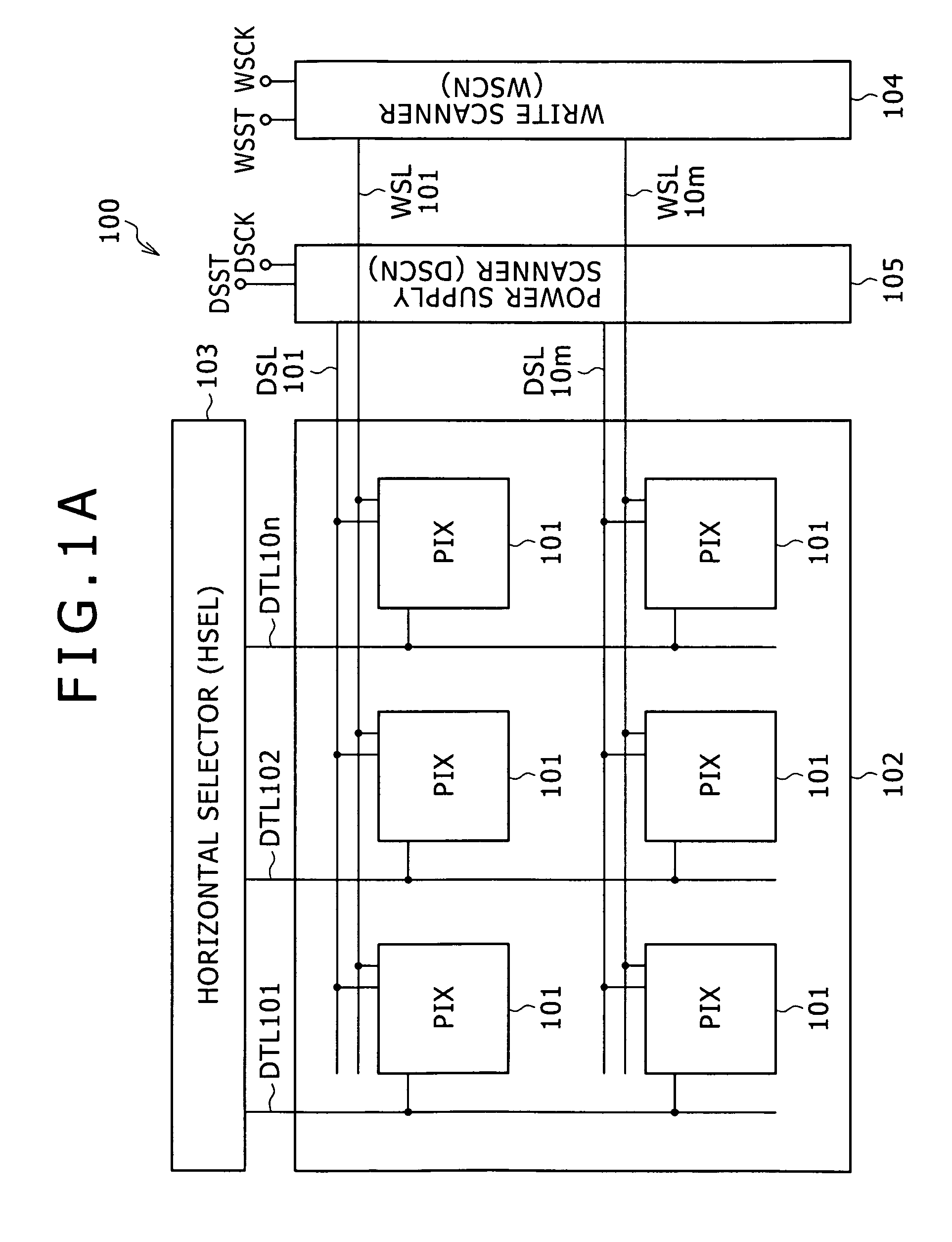
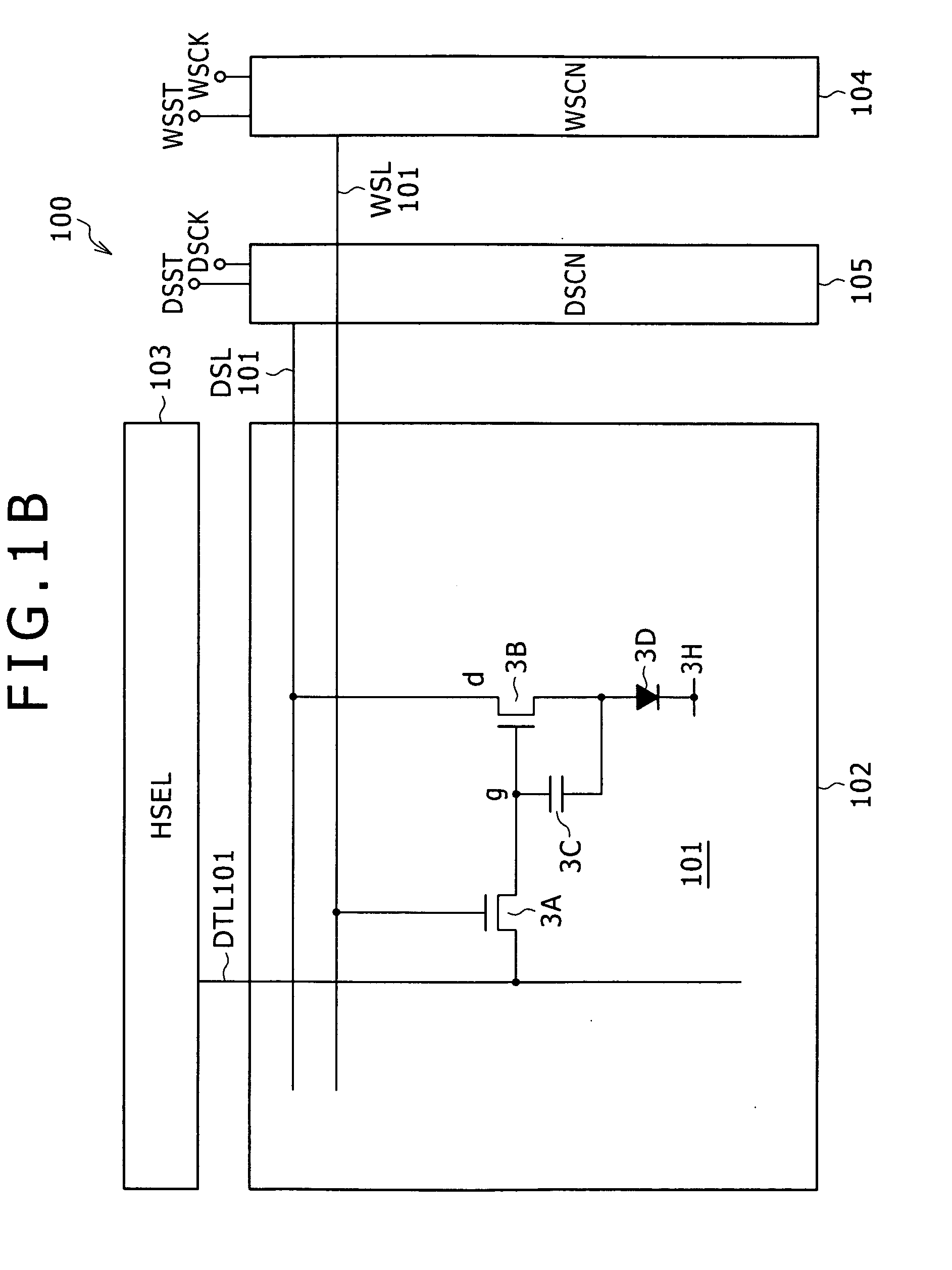
[0034]Embodiments of the present invention will be described in detail below with reference to the drawings. Initially, in order to clearly show the background of the present invention and facilitate understanding thereof, the general configuration of an active-matrix display device will be described below as a reference example. FIG. 1A is a block diagram showing the entire configuration of the display device according to the reference example. As shown in FIG. 1A, this display device 100 includes a pixel array part 102 and a drive part (103, 104, 105) for driving the pixel array part 102. The pixel array part 102 includes row scan lines WSL101 to WSL10m, column signal lines DTL101 to DTL10n, pixels (PIX) 101 disposed near the intersections of both the lines so as to be arranged in a matrix, and power feed lines DSL101 to DSL10m disposed corresponding to the respective rows of the pixels 101. The drive part (103, 104, 105) includes a main scanner (write scanner WSCN) 104, a power s...


PUM


Abstract

Disclosed herein is a display device including: a pixel array part including row first drive lines, row second drive lines, and column signal lines; and a drive part including a horizontal drive circuit, a first vertical drive circuit, and a second vertical drive circuit, wherein the first vertical drive circuit simultaneously drives pixels on two rows adjacent to each other, the second vertical drive circuit simultaneously drives pixels on two rows adjacent to each other, and a pair of rows of the pixels simultaneously driven by the first vertical drive circuit and a pair of rows of the pixels simultaneously driven by the second vertical drive circuit are shifted from each other by one row, for light-emission operation of the pixels on a row-by-row basis.

Description

CROSS REFERENCES TO RELATED APPLICATIONS[0001]The present invention contains subject matter related to Japanese Patent Application JP 2007-330803 filed in the Japan Patent Office on Dec. 21, 2007, the entire contents of which being incorporated herein by reference.BACKGROUND OF THE INVENTION[0002]1. Field of the Invention[0003]The present invention relates to an active-matrix display device including light-emitting elements in its pixels, and a method for driving the same. Furthermore, the present invention relates to an electronic apparatus in which such a display device is incorporated as a display or a monitor.[0004]2. Description of the Related Art[0005]In recent years, development of flat self-luminous display devices including organic EL (electroluminescence) devices as light-emitting elements is being actively promoted. The organic EL device is based on a phenomenon that an organic thin film emits light in response to application of an electric field thereto. The organic EL d...

Claims


Application Information

Patent Timeline
Patent Type & Authority Patents(United States)
IPC IPC(8): G09G5/00G09G3/34
CPCG09G3/3233G09G3/3275G09G2300/0819H01J37/2955H10K59/10
Inventor TANIKAME, TAKAO
Owner JOLED INC
Why Eureka
Try Eureka