Image display

a technology for image display and flexible substrates, applied in the direction of discharge tubes/lamp details, discharge tubes luminescnet screens, instruments, etc., can solve the problems of increasing the cost of members, affecting the practical application of the display panel, so as to prevent the substrate from fracturing

Active Publication Date: 2012-10-23
JAPAN DISPLAY INC +1
View PDF12 Cites 38 Cited by
  • Summary
  • Abstract
  • Description
  • Claims
  • Application Information

AI Technical Summary

Benefits of technology

[0015]An object of the present invention is to provide an image display which is capable of preventing fracturing of the substrate which is attributable to a substrate expansion arising from heating or humidification during a manufacture process, impact in use, or distortion when curved display is conducted, a connection failure between a semiconductor chip and a wiring terminal which are mounted on the substrate, and the crack occurring in the substrate in the vicinity of an area where a semiconductor chip is mounted, with no need to add the members and with no limit of pulling the wiring around.
[0016]The image display according to the present invention is configured to absorb a stress exerted on the substrate by a groove defined in the substrate (a recess having a depth not reaching a thickness of the substrate) so as to prevent the stress from being transmitted to an area other than the groove.
[0035]The image display configured as described above is capable of preventing fracturing of the substrate which is attributable to a substrate expansion arising from heating or humidification during a manufacture process, impact in use, or distortion when curved display is conducted, a connection failure between a semiconductor chip and a wiring terminal which are mounted on the substrate, and the crack occurring in the substrate in the vicinity of an area where a semiconductor chip is mounted, with no need to add the members and with no limit of pulling the wiring around.

Problems solved by technology

However, a display panel using the flexible substrate is subjected to a stress attributed to various factors such as substrate expansion arising from heating or humidification during a manufacture process, impact in use, and distortion when curved display is conducted.
Because the stress leads to such a problem that the flexible substrate is fractured, the stress becomes a major issue for practical application.
In addition to fracturing of the substrate, it is confirmed that there occurs a connection failure between a semiconductor chip and a wiring terminal which are mounted on the substrate, and the substrate cracks in the vicinity of an area where a semiconductor chip is mounted.
The former problem with the substrate fracturing is recently revealed, but the latter problem with the connection failure of the semiconductor chip and crack of the peripheral substrate has been known in the pasts.
However, the provision of the flexible substrate independently from the display panel as in the related art increases the member costs as much, and also requires the process costs for the cramping process.
Also, the liquid crystal image display disclosed in JP-A-2003-114433 is complicated in a cutting process, and further the formed strip part is slender.
This leads to such a problem that the treatment is difficult.
Also, the flexible display disclosed in JP-A-2005-331914 is complicated in a notching process as in JP-A-2003-114433, and also requires that a wiring between the image display region and the semiconductor chip is pulled around so as to avoid the part where the notch is formed.

Method used


Image

  • Image display
  • Image display
  • Image display

Examples


first embodiment

[First Embodiment]

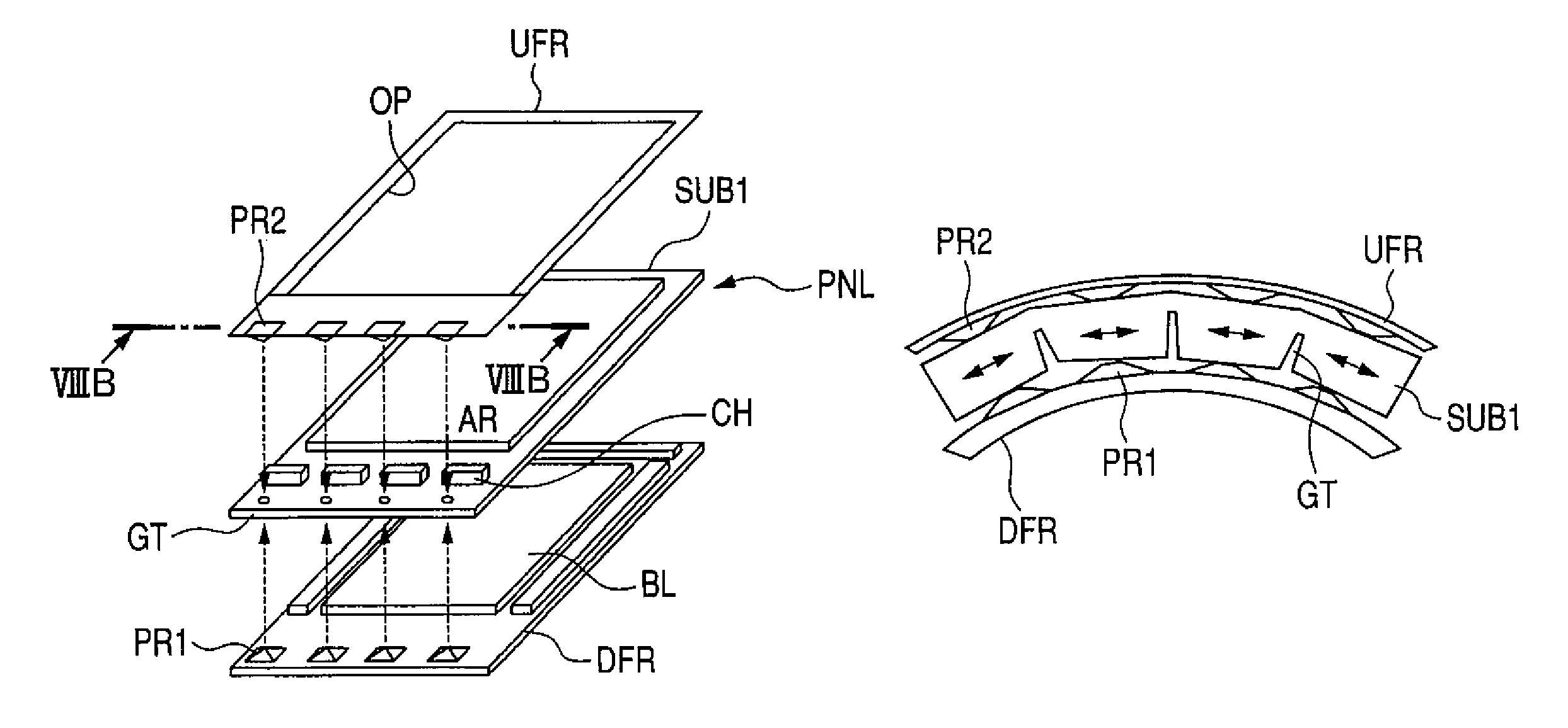
[0048]FIGS. 1A and 1B are configuration diagrams showing an image display according to a first embodiment of the present invention, respectively. FIG. 1A is a plan view, and FIG. 1B is a cross-sectional view taken along a line IB-IB of FIG. 1A.

[0049]First, a flexible substrate SUB1 is made of, for example, a resin material, and a so-called TFT layer PLL is formed on a surface of the substrate SUB1 at an image display part AR side. The TFT layer PLL is formed of a laminated body in which an insulating film, a semiconductor layer, and a metal film are laminated on one another in a given order in a given pattern to configure an electronic circuit necessary for image display. Although not shown, the TFT layer PLL is, for example, deposited on a surface of the substrate SUB1 via an adhesive layer. This is because there is employed a technique by which after the TFT layer PLL has been formed on a provisional substrate made of glass having heat resistance and rigidity, th...

second embodiment

[Second Embodiment]

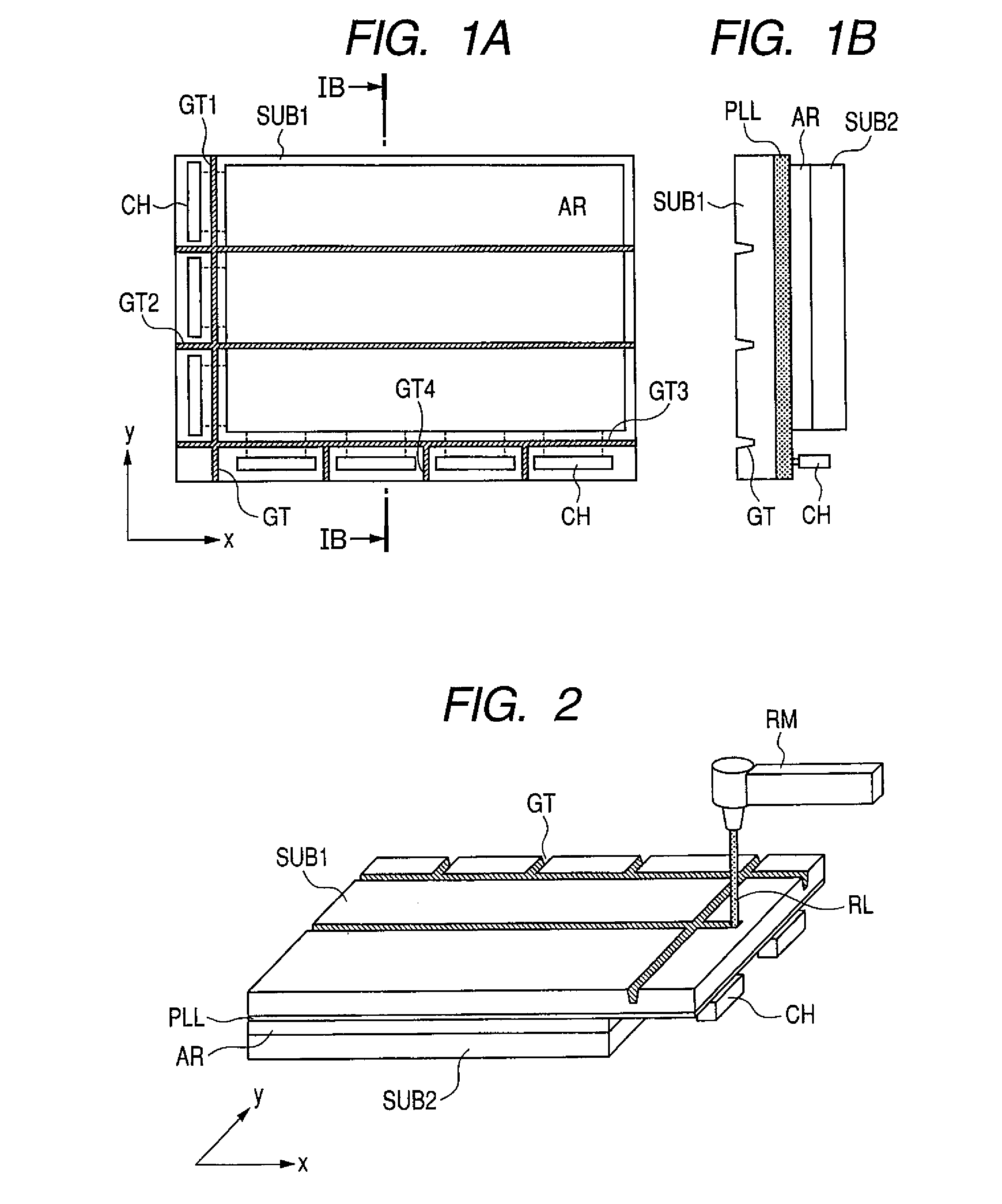
[0064]FIG. 4A is a configuration diagram showing an image display according to a second embodiment of the present invention.

[0065]Referring to FIG. 4A, configurations different from that in the case of FIG. 1A reside in that the number of grooves GT is three, and the entire panel is divided into four smaller areas. When the number of grooves GT along a given direction is thus increased, there is advantageous in that the stress can be reduced when the curvature is smaller in the radius of curvature. The radius of curvature which can be dealt with is smaller as the number of grooves GT is larger. On the other hand, there is disadvantageous in that the strength of the entire panel is reduced, and the costs of a process for forming a larger number of grooves GT increase. For that reason, an appropriate number of grooves GT may be set according to the use condition. Accordingly, the number of grooves GT is not limited to three or four.

third embodiment

[Third Embodiment]

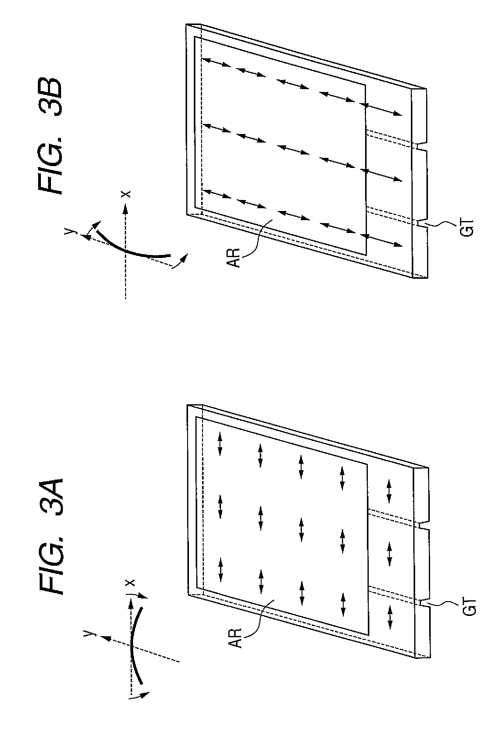
[0066]FIG. 4B is a configuration diagram showing an image display according to a third embodiment of the present invention.

[0067]Referring to FIG. 4B, configurations different from that in the case of FIG. 4A reside in that the grooves GT defined to divide and surround the respective areas are not continuous, but partially intermittent grooves are added together in the x-direction and the y-direction. In this case, even if the impact or curvature to be applied to the panel is in both of the x-direction and the y-direction, there is advantageous in that a part of the intermittent grooves GT can always absorb the stress. Therefore, the strength of the entire panel can be improved under an environment where a direction of the stress is not determined in advance. Further, because, in addition to the curvature in one direction, a curvature in a direction perpendicular to the one direction is enabled at some level, a display method in which curvature is made in both of t...


PUM

PropertyMeasurementUnit
stressaaaaaaaaaa
distortion stressaaaaaaaaaa

Abstract

To provide an image display which is capable of preventing fracturing of a substrate which is attributable to a substrate expansion arising from heating or humidification during a manufacture process, impact in use, or distortion when curved display is conducted, a connection failure between a semiconductor chip and a wiring terminal which are mounted on the substrate, and crack occurring in the substrate in the vicinity of an area where the semiconductor chip is mounted, with no need to add members and with no limit of pulling the wiring around. An image display part is formed on one surface of a flexible substrate, and a groove with a depth not reaching a thickness of the substrate is continuously or intermittently defined in another surface of the substrate.

Description

CLAIM OF PRIORITY[0001]The present application claims priority from Japanese patent application JP 2008-240272 filed on Sep. 19, 2008, the content of which is hereby incorporated by reference into this application.BACKGROUND OF THE INVENTION[0002]1. Field of the Invention[0003]The present invention relates to an image display, and more particularly to an image display having a flexible substrate made of, for example, a resin material.[0004]2. Description of the Related Art[0005]In recent years, there has been known a flexible display using a flexible substrate made of, for example, a resin material instead of a conventional glass substrate. This is because the use of the flexible substrate improves thinning, weight saving, impact resistance, and curved display property of the image display.[0006]However, a display panel using the flexible substrate is subjected to a stress attributed to various factors such as substrate expansion arising from heating or humidification during a manuf...

Claims


Application Information

Patent Timeline
Patent Type & Authority Patents(United States)
IPC IPC(8): G02F1/1333
CPCG02F1/133305G02F1/13452
Inventor YAMAGUCHI, SHINYAHATANO, MUTSUKOHATTORI, TAKASHIOKADA, NAOYA
Owner JAPAN DISPLAY INC
Why Eureka
Try Eureka