Semiconductor device having IGBT and FWD on same substrate

a technology of igbt and fwd, which is applied in the direction of semiconductor devices, basic electric elements, electrical appliances, etc., can solve the problems of large area for functioning anodes, and achieve the effect of reducing the on-state voltage of igbt and the forward voltage of fwd

Active Publication Date: 2012-10-30
DENSO CORP
View PDF26 Cites 17 Cited by
  • Summary
  • Abstract
  • Description
  • Claims
  • Application Information

AI Technical Summary

Benefits of technology

[0008]In view of the above-described problem; it is an object of the present disclosure to provide a semiconductor device having an IGBT and a FWD, which are arranged on the same semiconductor substrate. In the device, a chip size of the device is improved, and a forward voltage of the FWD and an on-state voltage of the IGBT are improved.
[0011]Further, the part of the cathode side second region is electrically coupled with the emitter electrode. Thus, the part of the cathode side second region together with the first regions function as an anode of the FWD element. Thus, the area for functioning the anode becomes large. Further, current path of the FWD is shortened. Furthermore, since the emitter region of the IGBT does not exist in the second region, even when the driving signal is input into the gate electrode, the second region and the substrate do not have the same potential. Thus, the second region is not affected by the influence of the gate electrode. Accordingly, the forward voltage of the FWD is reduced.

Problems solved by technology

Thus, the area for functioning the anode becomes large.

Method used


Image

  • Semiconductor device having IGBT and FWD on same substrate
  • Semiconductor device having IGBT and FWD on same substrate
  • Semiconductor device having IGBT and FWD on same substrate

Examples


first embodiment

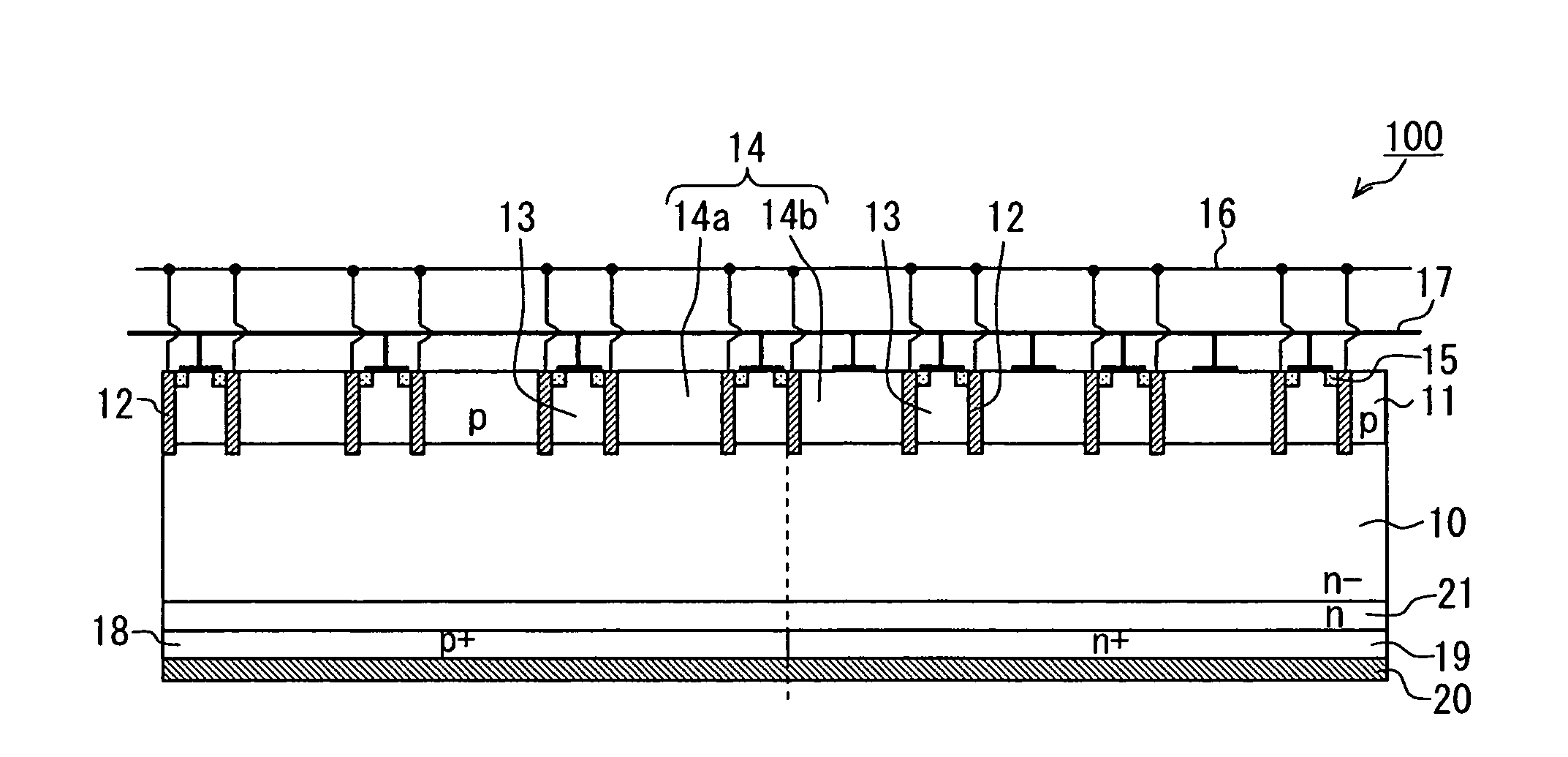
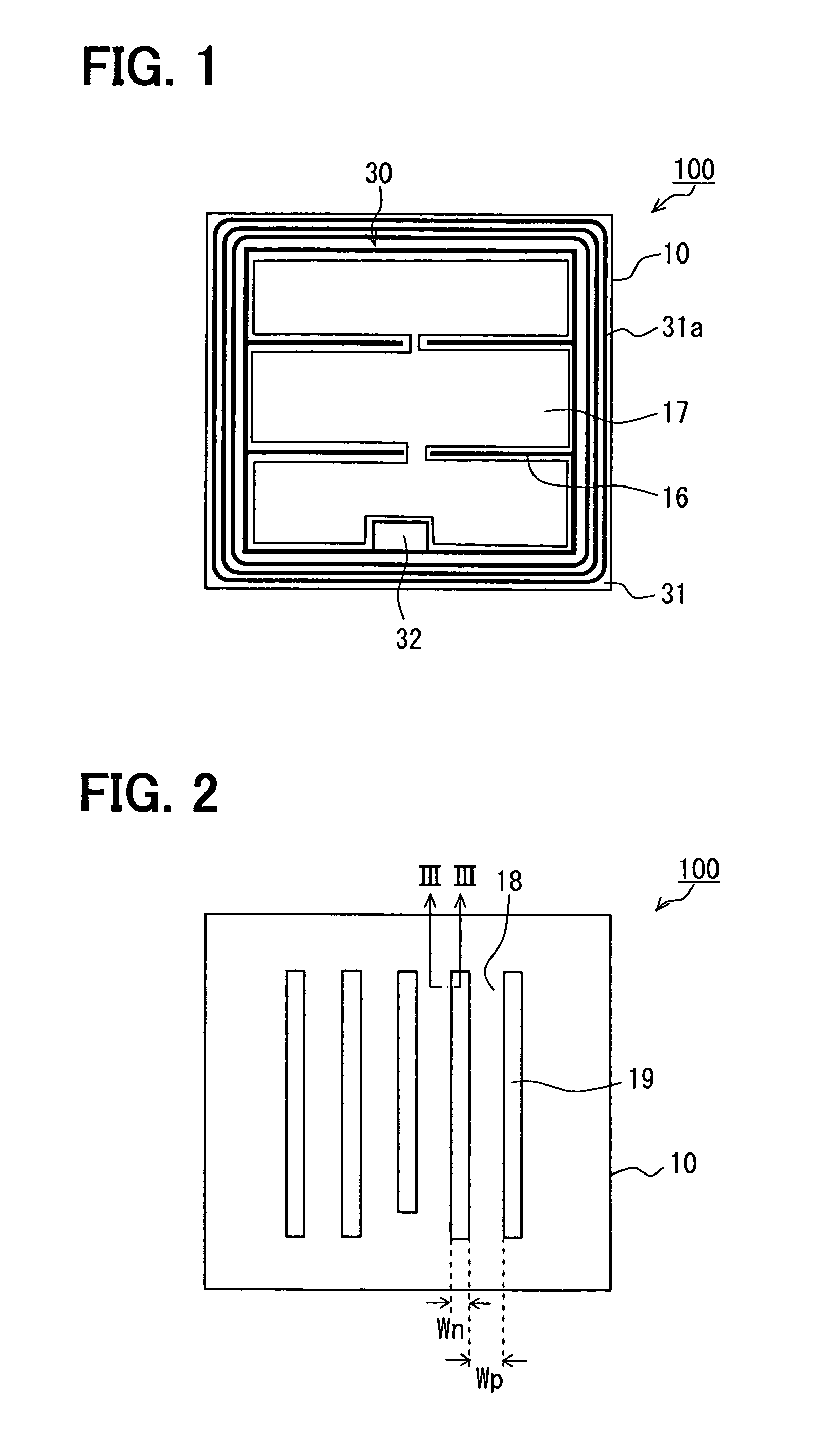
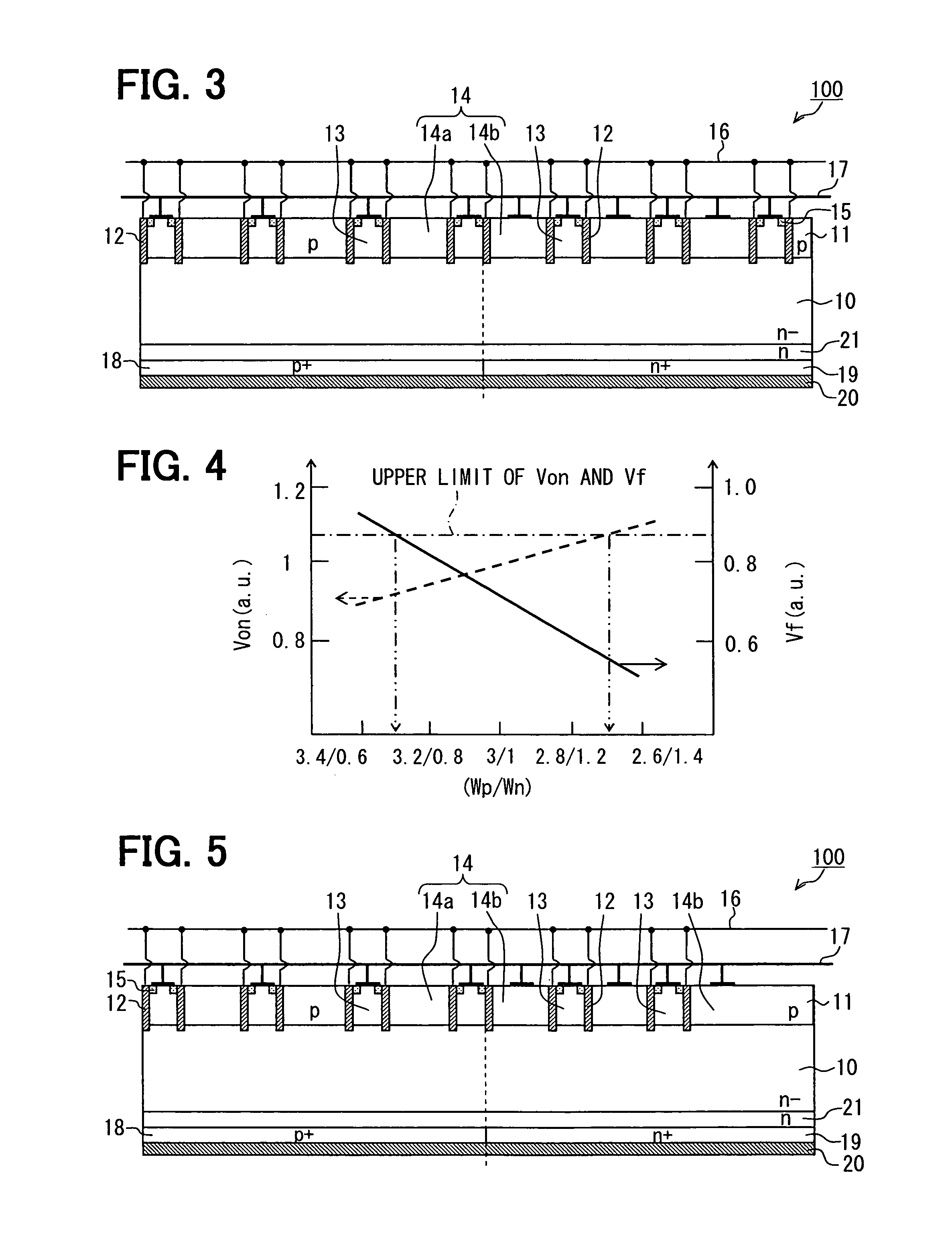
[0046]FIGS. 1-3 show a semiconductor device according to a first embodiment. In FIG. 2, a collector electrode of the device is not shown.

[0047]The semiconductor device is suitably used for a power switching device in an inverter module of an EHV (electric and hybrid vehicle). Here, a thickness direction of a semiconductor substrate is perpendicular to the substrate, and one direction perpendicular to the thickness direction is defined as a parallel direction of the substrate. The parallel direction is in parallel to a direction of arrangement of a collector region and a cathode region. A N conductive type is, for example, a first conductive type, and a P conductive type is a second conductive type. Alternatively, the first conductive type may be the P conductive type, and the second conductive type may be the N conductive type.

[0048]The device 100 in FIGS. 1-3 includes a semiconductor substrate 10 having the first conductive type. The substrate 10 includes a region 30, in which an I...

second embodiment

[0071]FIG. 5 shows a semiconductor device 100 according to a second embodiment.

[0072]In FIG. 3, the first region 13 having the emitter region 15 in the surface portion of the first region 13 is arranged directly over the collector region 18 and the cathode region 19. The forming area of the first region 13 is not specified. For example, multiple first regions 13 are repeatedly arranged at predetermined intervals along with the parallel direction.

[0073]In FIG. 5, the gate electrode 12 and the first region 13 are formed in a part of the base layer 11 directly over the cathode region 19. Specifically, they are formed from a boundary between the cathode region 19 and the collector region 18 to a predetermined range of the cathode region 19. The cathode side second region 14b is formed in the other part of the base layer 11 over the cathode region 19. The device in FIG. 5 is formed as follows. Specifically, in FIG. 3, one of three first regions 13 over the cathode region 19 is removed. T...

third embodiment

[0078]FIG. 6 shows a semiconductor device according to a third embodiment.

[0079]The gate electrode 12 and the first region 13 are formed only in a part of the base layer 11 disposed directly over the cathode region 19. The part of the base layer 11 is disposed in a predetermined range from an interface between the cathode region 19 and the collector region 18. The interface is defined as a broken line in FIG. 6. The part of the base layer 11 is defined as an adjacent region of the collector region 18. Multiple dummy gate electrodes 22 are formed in the other part of the base layer 11 over the cathode region 19. The dummy gate electrode 22 has the same potential as the gate electrode 12, and is made of the same material as the gate electrode 12. Further, the dummy gate electrode 22 has the same structure as the gate electrode 12. The cathode side second region 14b is formed in a region sandwiched between a pair of dummy gate electrodes 22. The second region 14b sandwiched between a p...


PUM


Abstract

A semiconductor device includes: a semiconductor substrate; an IGBT element including a collector region; a FWD element including a cathode region adjacent to the collector region; a base layer on the substrate; multiple trench gate structures including a gate electrode. The base layer is divided by the trench gate structures into multiple first and second regions. Each first region includes an emitter region contacting the gate electrode. Each first region together with the emitter region is electrically coupled with an emitter electrode. The first regions include collector side and cathode side first regions, and the second regions include collector side and cathode side second regions. At least a part of the cathode side second region is electrically coupled with the emitter electrode, and at least a part of the collector side second region has a floating potential.

Description

CROSS REFERENCE TO RELATED APPLICATIONS[0001]This application is based on Japanese Patent Applications No. 2008-265593 filed on Oct. 14, 2008, and No. 2009-162041 filed on Jul. 8, 2009, the disclosures of which are incorporated herein by reference.FIELD OF THE INVENTION[0002]The present invention relates to a semiconductor device having an IGBT and a FWD, which are arranged on the same semiconductor substrate.BACKGROUND OF THE INVENTION[0003]Conventionally, for example as disclosed in JP-2005-317751 corresponding to US 2005 / 0258493, a reverse conduction type semiconductor device (i.e., RC-IGBT or reverse conducting IGBT) includes an IGBT (insulated gate bipolar transistor) and a FWD (free wheel diode), which are disposed in the same semiconductor substrate, so that the FWD is built in the IGBT.[0004]In the RC-IGBT, an anode electrode of the FWD and an emitter electrode of the IGBT are common, and a cathode electrode of the FWD and a collector electrode of the IGBT are common. The RC...

Claims


Application Information

Patent Timeline
Patent Type & Authority Patents(United States)
IPC IPC(8): H01L27/06
CPCH01L29/7395H01L29/861H01L2224/0603
Inventor KOUNO, KENJI
Owner DENSO CORP
Why Eureka
Try Eureka