

Semiconductor memory device
a memory device and semiconductor technology, applied in the field of semiconductor memory devices, can solve the problems of increasing the circuit area, increasing the switching time and the operation time,
- Summary
- Abstract
- Description
- Claims
- Application Information
AI Technical Summary
Benefits of technology
Problems solved by technology
Method used
Image

Examples
first embodiment
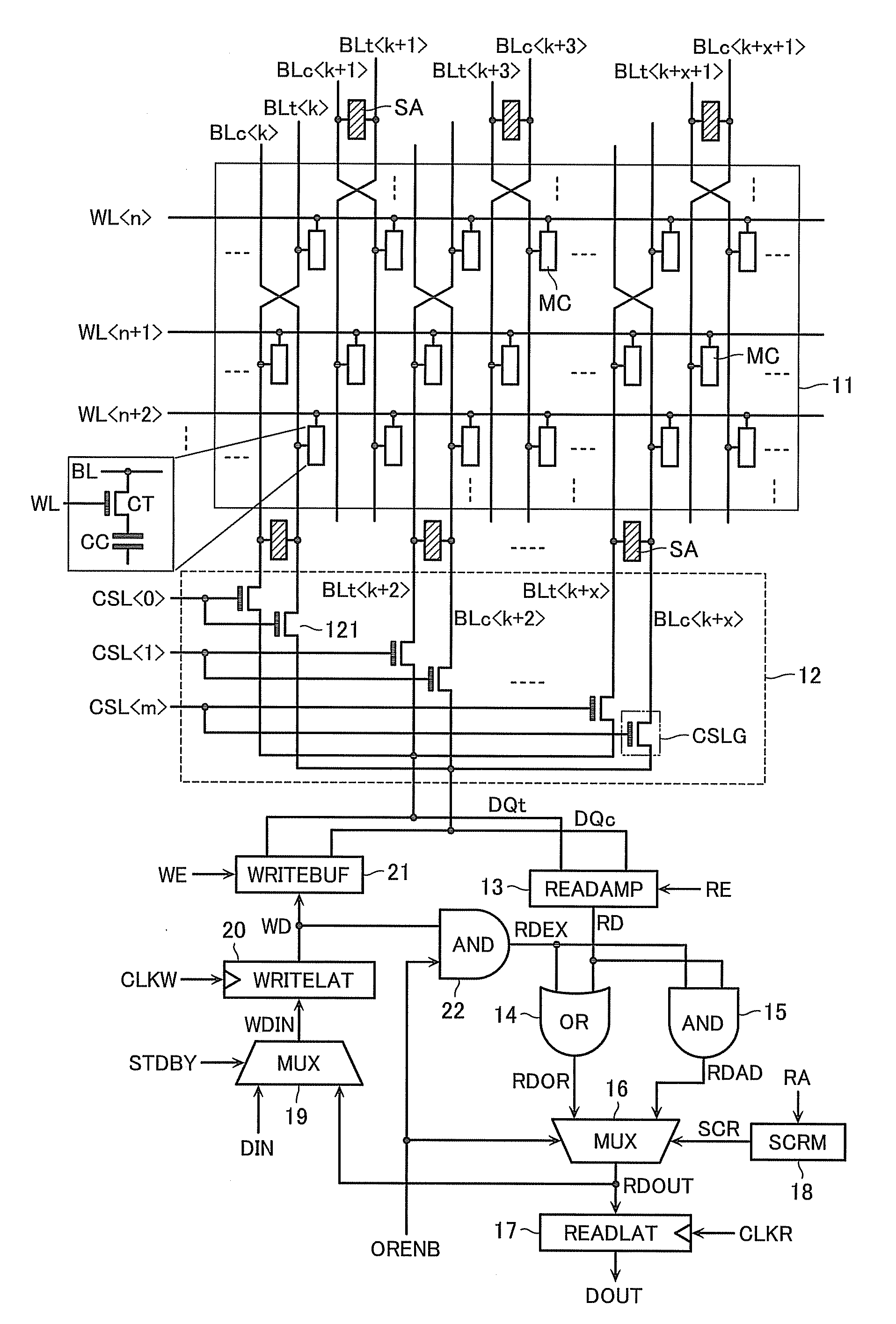
[0018]First, with reference to FIG. 1, a DRAM according to a first embodiment of the present invention is described below. The DRAM includes a memory cell array 11 and a column gate 12.
[0019]The memory cell array 11 includes memory cells MC in a matrix at intersections of word-lines WL and bit-lines BL. By way of example, the memory cell MC includes one cell-capacitor CC and one cell-transistor CT that are connected in series. The memory cell MC stores data using a charge (not shown) held in the cell capacitor CC.
[0020]In the bit-lines BL, a bit-line BLt and a bit-line BLc compose a complementary bit-line pair. Each complementary bit-line pair has a sense amplifier circuit SA formed therebetween. FIG. 1 shows a DRAM that utilizes the so-called folded bit-line structure. In the structure, the bit-line BLt and the bit-line BLc composing a complementary bit-line pair are provided in the same memory cell array 11. The bit-line BLt and the bit-line BLc form a twisted bit-line structure i...
second embodiment
[0050]With reference now to FIG. 5, a DRAM configuration according to a second embodiment of the present invention will be described below. The entire configuration of this embodiment is generally the same as that of the DRAM in FIG. 1. This embodiment differs, however, from the first embodiment in that data of the copy-source memory cell MCo is copied to the copy-destination memory cell MCc using an additional transfer gate circuit for copy operation 23. The transfer gate circuit for copy operation 23 includes one nMOS transistor connected between the bit-line BLt and the bit-line BLt. The nMOS transistor forms a current path between the two bit-lines. The nMOS transistor is rendered conductive by the raising of the control signal MUXCP to “H.” When the signal read from the copy-source memory cell MCo is amplified by the sense amplifier circuit SA and appears on the bit-line BLt, the transfer gate circuit for copy operation 23 rendered conductive transfers a voltage corresponding t...
third embodiment
[0054]With reference to FIG. 7, a third embodiment of the present invention will be described below. In FIG. 7, like elements as those of the DRAM in the first embodiment are designated by like reference numerals as those in FIG. 1, and their detailed description is omitted here. The DRAM in this embodiment differs from that in the first embodiment in that data is not scrambled before it is written to the memory cell array 11 and thus the scramble control circuit 18 is omitted. Because the scramble control is not performed, the AND gate 15 is omitted and the logic operation of data of the copy-source memory cell MCo and data of the copy-destination memory cell MCc is performed only by the OR gate 14. The other points are similar to those in the first embodiment.
[0055]FIGS. 8 and 9 are timing diagrams for reading data in the twin-cell configuration in this embodiment. FIGS. 8 and 9 are similar to FIGS. 3 to 5 except that the scramble control signal SCR is not used, and thus their det...
PUM
 Abstract
Description
Claims
Application Information