Composite electronic device

a technology of electronic devices and composite materials, applied in the direction of overvoltage protection resistors, emergency protective arrangements for limiting excess voltage/current, and arrangements responsive to excess voltage, can solve the problems of large esd (electrostatic discharge) problem, signal waveform becomes inert, circuit generates relatively large radiation electromagnetic field, etc., to achieve excellent discharge characteristics, small electrostatic capacitance, and easy manufacturing. effect of tim

Active Publication Date: 2012-11-27
TDK CORPARATION
View PDF15 Cites 7 Cited by
  • Summary
  • Abstract
  • Description
  • Claims
  • Application Information

AI Technical Summary

Benefits of technology

[0010]Therefore, it is an object of the present invention to provide a compact and high-performance composite electronic device constituted by combining a common mode filter and ESD protection elements having a small electrostatic capacitance and excellent discharge characteristic, heat resistance, and weatherability.

Problems solved by technology

However, this circuit generates a relatively large radiation electromagnetic field when common noise (common mode noise) is superimposed on the signal lines 1 and 2.
Accordingly, ESD (electrostatic discharge) becomes a large problem.
However, when the varistor is used, a signal waveform becomes inert, and signal quality is degraded.
Therefore, the ESD protection elements need to be provided on the uppermost part due to a constraint of a manufacturing step which becomes a large constraint on design.
Consequently, it is considerably difficult to stably form a very fine gap.
Further, in forming the ESD protection elements on a top layer, the manufacturing step becomes complex, and manufacturing cost increases.

Method used


Image

  • Composite electronic device
  • Composite electronic device
  • Composite electronic device

Examples


first embodiment

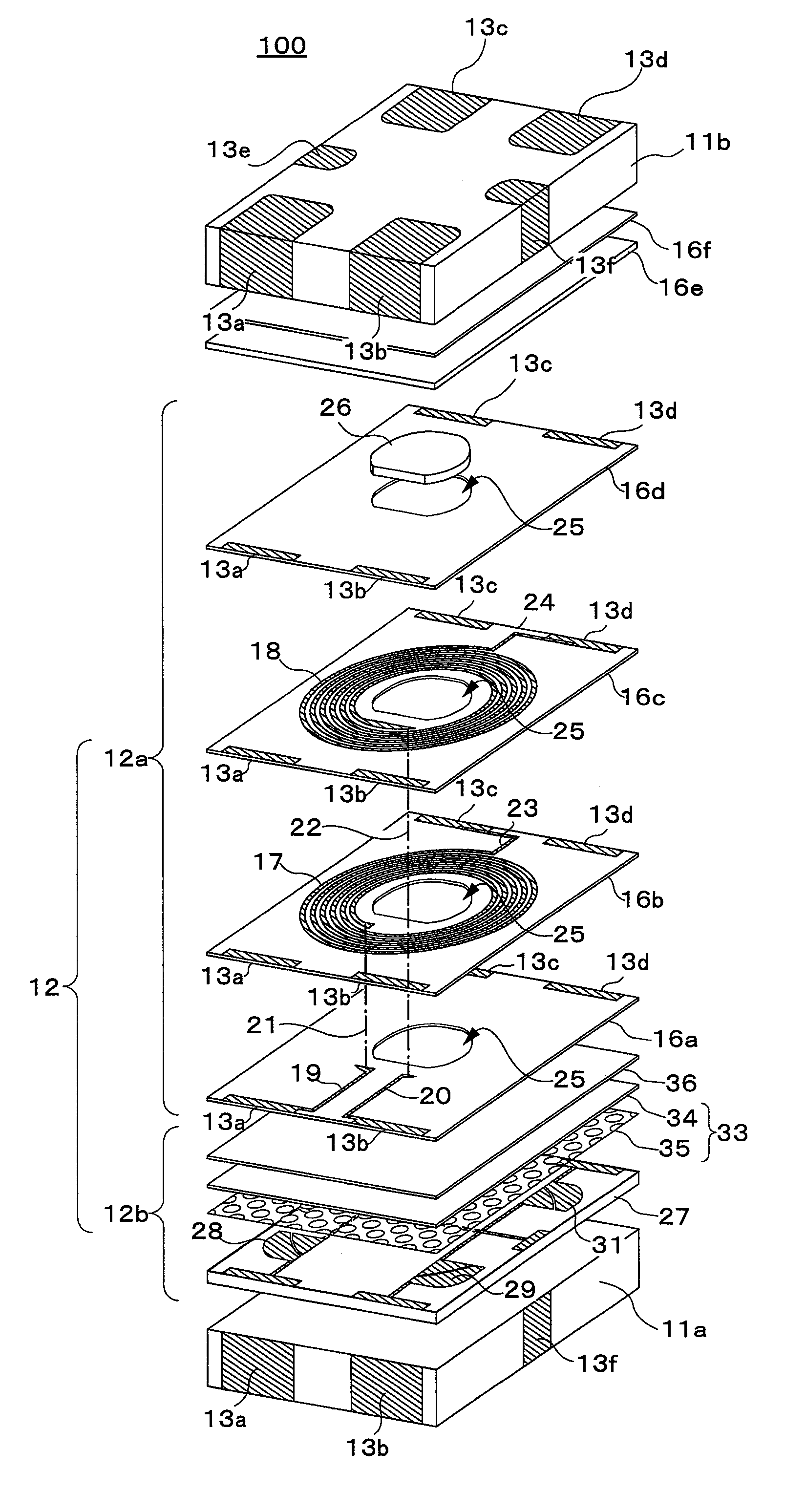
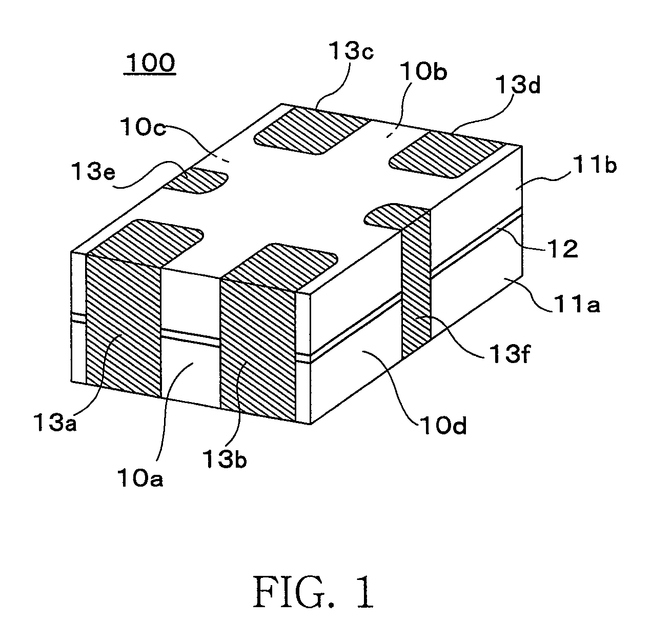
[0042]FIG. 1 is a schematic perspective view showing an external configuration of a composite electronic device 100 according to the present invention.

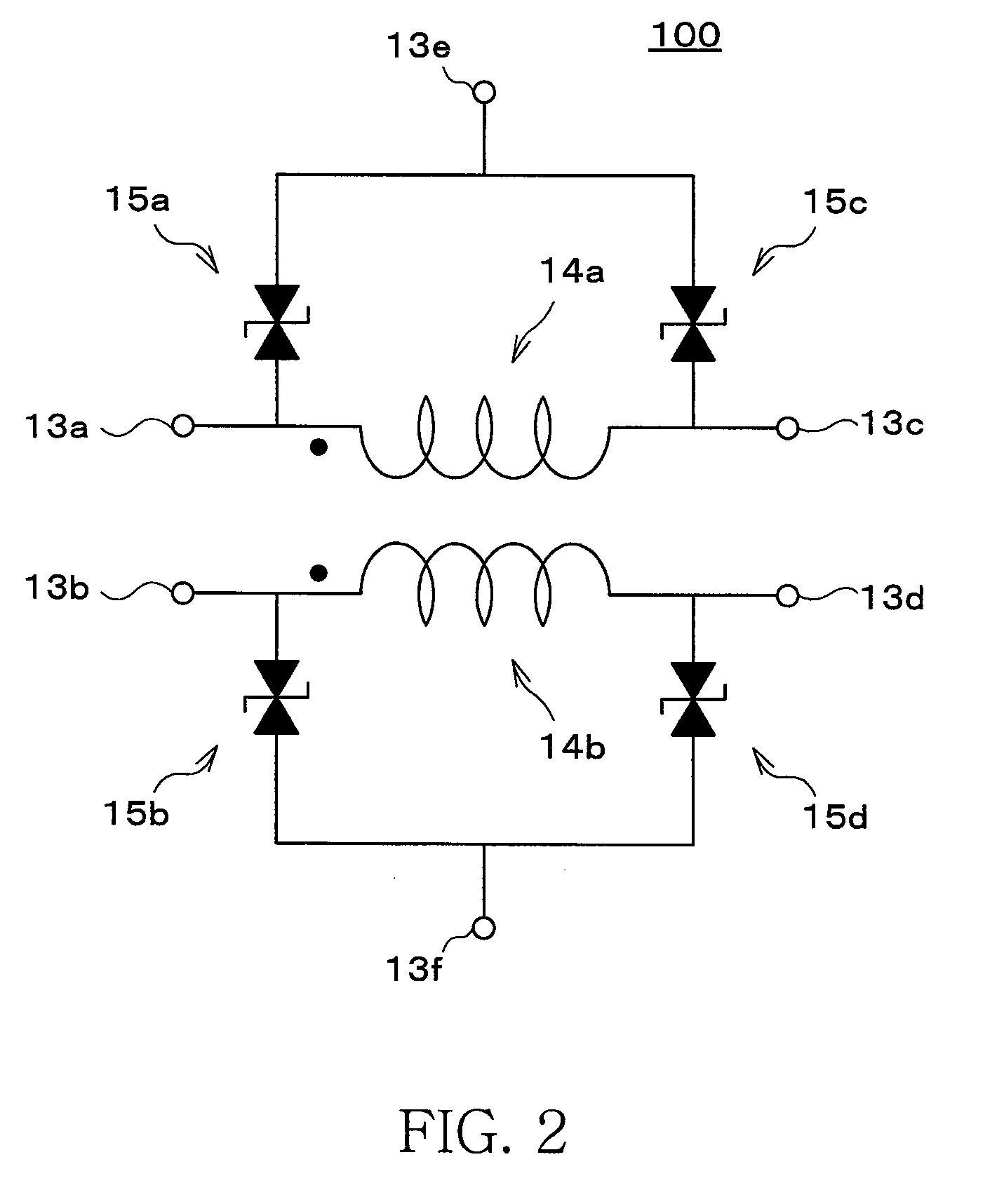
[0043]As shown in FIG. 1, the composite electronic device 100 according to the first embodiment is a thin-film common mode filter having an ESD protection function, and includes first and second magnetic substrates 11a and 11b, and a function layer 12 sandwiched between the first magnetic substrate 11a and the second magnetic substrate 11b. First to sixth terminal electrodes 13a to 13f are formed on an external peripheral surface of a laminated body constituted by the first magnetic substrate 11a, the function layer 12, and the second magnetic substrate 11b. The first and second terminal electrodes 13a and 13b are formed on a first side surface 10a orthogonal with longitudinal direction of the laminated body. The third and fourth terminal electrodes 13c and 13d are formed on a second side surface 10b opposite to the first side surface...

second embodiment

[0102]FIG. 8 is a schematic plan view transparently showing the structure of a composite electronic device 200 according to the present invention.

[0103]As shown in FIG. 8, a composite electronic device 200 according to the second embodiment is characterized in that the entire of each gap electrodes 28 to 31 are provided at positions not overlapped on the spiral conductors 17 and 18. Since other configurations are the same as the composite electronic device 100 according to the first embodiment, the same reference numerals are used for the same constituent elements, and a description thereof is omitted.

[0104]When the spiral conductors 17 and 18 are disposed in the above way, a wider mounting area is needed and a chip size needs to be slightly increased. However, the same function and effect as those of the first embodiment can be achieved. That is, the formation positions of the gaps are closer to the outside than the outermost circumferences of the spiral conductors 17 and 18, and t...

third embodiment

[0105]FIG. 9 is a schematic plan view transparently showing the structure of a composite electronic device 300 according to the present invention.

[0106]As shown in FIG. 9, the composite electrode device 300 of this embodiment is characterized in that the spiral conductors is not an approximately round spiral conductor (a circular pattern formed by a curved line), but an approximately rectangular spiral conductor (an angle pattern formed by straight lines). Since other configurations are the same as the composite electronic device 100 according to the first embodiment, the same reference numerals are used for the same constituent elements, and a description thereof is omitted.

[0107]As such, the spiral shape and the gap shape of the composite electrode device 300 are different from those of the composite electronic device 100, but the same function and effect as those of the first embodiment can be achieved. That is, the formation positions of the gaps are closer to the outside than t...


PUM


Abstract

The present invention is provided with a composite electronic device comprising an inductor element and an ESD protection element formed between two magnetic substrates, wherein the inductor element includes insulation layers made of a resin, and spiral conductors formed on the insulation layers, the ESD protection element includes a base insulation layer, a pair of gap electrodes arranged via gap formed therebetween on the base insulation layer, and an ESD absorbing layer arranged at least between the gap electrodes, and the ESD absorbing layer includes a composite material having an insulation inorganic material and a conductive inorganic material discontinuously dispersed in a matrix of the insulation inorganic material. The gap of the ESD protection element is provided at exterior of the spiral conductor so as not to be overlapped with the spiral conductor in view of a laminating direction.

Description

TECHNICAL FIELD[0001]The present invention relates to a composite electronic device, and, more particularly relates to a structure of a composite electronic device constituted by combining inductor elements and electrostatic discharge (ESD) protection elements.BACKGROUND OF THE INVENTION[0002]In recent years, standards of USB 2.0 and a high-definition multimedia interface (HDMI) have been widely distributed as high-speed signal transmission interfaces, and they are used in many digital devices such as personal computers and digital high-vision televisions. These interfaces employ a differential signal system that transmits a differential signal (a differential mode signal) by using a pair of signal lines, unlike a single-end transmission system that has been generally used for many years.[0003]The differential transmission system has excellent characteristics in that the system is not easily affected by exogenous noise as well as that the system has a small radiation electromagnetic...

Claims


Application Information

Patent Timeline
Patent Type & Authority Patents(United States)
IPC IPC(8): H01C7/12
CPCH03H7/0107H03H7/427H03H2001/0085
Inventor ASAKAWA, MASAOITO, TOMOKAZUNAKAGOMI, SHOHITOMI, ATSUSHIHIROBE, YASUHIROASAKURA, KENSAKU
Owner TDK CORPARATION
Why Eureka
Try Eureka