Semiconductor device and IC label, IC tag, and IC card provided with the semiconductor device

a semiconductor device and semiconductor technology, applied in the field of semiconductor devices, can solve the problems of difficult to accumulate inputted charges, take long to obtain a desired voltage, etc., and achieve the effect of large electric charge accumulation circuit capacitance and efficient accumulation

Inactive Publication Date: 2011-10-11
SEMICON ENERGY LAB CO LTD
View PDF68 Cites 4 Cited by
  • Summary
  • Abstract
  • Description
  • Claims
  • Application Information

AI Technical Summary

Benefits of technology

[0010]In view of the aforementioned problems, an object of the present invention is to provide a semiconductor device capable of generating a desired voltage in a short time and applying a stable voltage to a constant voltage circuit.
[0011]To achieve the above object, the semiconductor device of the present invention is provided with a charge accumulation circuit having a structure in which a capacitor is divided into a plurality of pieces and the divided capacitors are connected in parallel through switches. Further, the charge accumulation circuit in the semiconductor device of the present invention controls the switches provided between the capacitors and thus can dynamically vary electrostatic capacitance of the charge accumulation circuit which applies a voltage to a constant voltage circuit.
[0016]The semiconductor device of the present invention includes a charge accumulation circuit which controls the switches between the capacitors provided separately. Thus, since the semiconductor device of the present invention can control the switch so that electrostatic capacitance of the charge accumulation circuit is small in an initial state in which energy is not accumulated, a desired voltage can be generated in a short period. Since the semiconductor device of the present invention can control the switches so that electrostatic capacitance of the charge accumulation circuit is large after the desired power supply voltage is obtained, inputted charges can be efficiently accumulated and a stable voltage can be applied to the constant voltage circuit.

Problems solved by technology

However, with high electrostatic capacitance of the capacitor, there is a problem in that it takes long to obtain a desired voltage by the time for accumulating charges in the capacitor.
Meanwhile, with low electrostatic capacitance of the capacitor, while a desired voltage can be obtained, there is a problem in that it becomes difficult to accumulate inputted charges and to apply a stable voltage to the constant voltage circuit of the next stage.

Method used


Image

  • Semiconductor device and IC label, IC tag, and IC card provided with the semiconductor device
  • Semiconductor device and IC label, IC tag, and IC card provided with the semiconductor device
  • Semiconductor device and IC label, IC tag, and IC card provided with the semiconductor device

Examples


embodiment mode 1

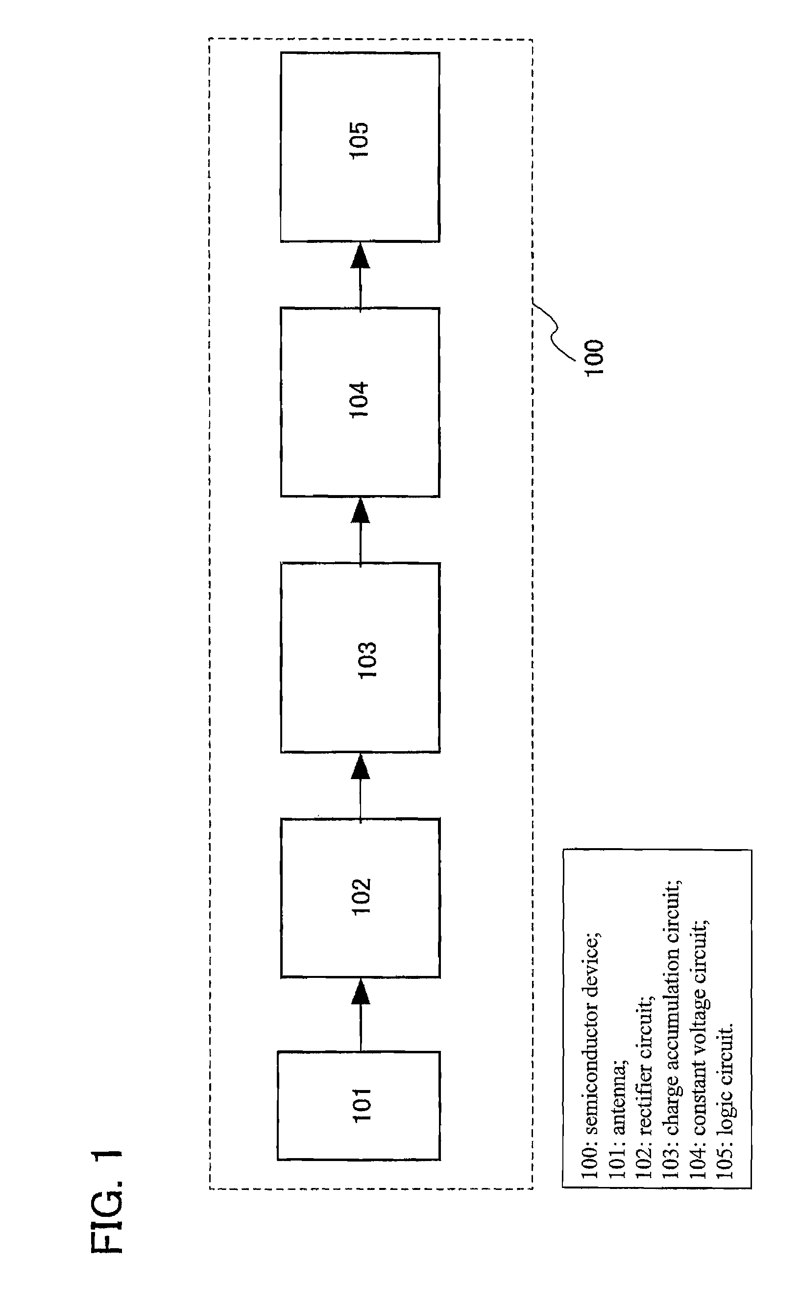
[0038]The structure of a semiconductor device of the present invention is described with reference to a block diagram shown in FIG. 1. Note that in this embodiment mode, the case is described in which the semiconductor device of the present invention is used as a semiconductor device capable of wirelessly communicating data, a so-called IC chip (also referred to as an ID chip, an IC chip, or a transponder) for RFID (radio frequency identification).

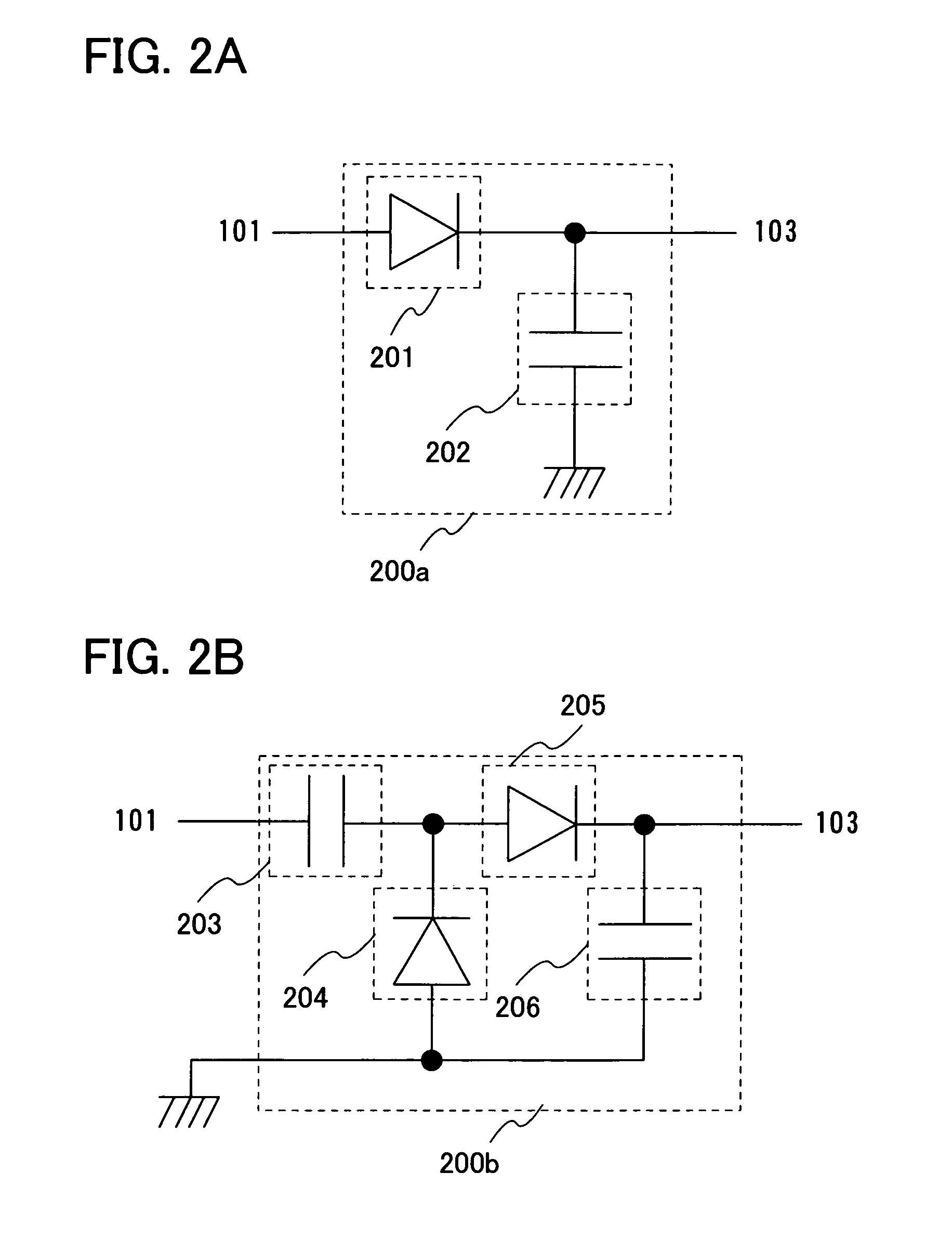
[0039]A semiconductor device 100 in FIG. 1 includes an antenna 101, a rectifier circuit 102, a charge accumulation circuit 103, a constant voltage circuit 104, and a logic circuit 105.

[0040]Note that although not shown here, the antenna 101 in FIG. 1 receives a signal from an external communication device (hereinafter referred to as a communication device, and also referred to as a reader / writer, a controller, or an interrogator) and transmits a signal to the communication device.

[0041]Note that the shape of the antenna 101 is not particul...

embodiment mode 2

[0072]In this embodiment mode, the structure of the semiconductor device provided with a charge accumulation circuit (also called an RFID tag, an ID chip, an IC tag, an ID tag, an RF tag, a wireless tag, an electronic tag, or a transponder), which is described in the above embodiment mode, is described.

[0073]A semiconductor device 800 in FIG. 8 includes, as an example, an antenna 801, a rectifier circuit 802, a charge accumulation circuit 803, a constant voltage circuit 804, a demodulation circuit 805, a modulation circuit 806, and a logic circuit 807. The logic circuit 807 includes a controller 808, a CPU (central processing unit) 809, a ROM 810 (read only memory) 810, and a RAM 811 (random access memory) 811. The logic circuit 807 is allowable as long as it includes a logic circuit such as the CPU 809, a volatile memory (typically, SRAM) as the RAM 811 serving as a work region, and a nonvolatile memory (typically, EEPROM) as the programmable ROM 810 which stores a program of the C...

embodiment mode 3

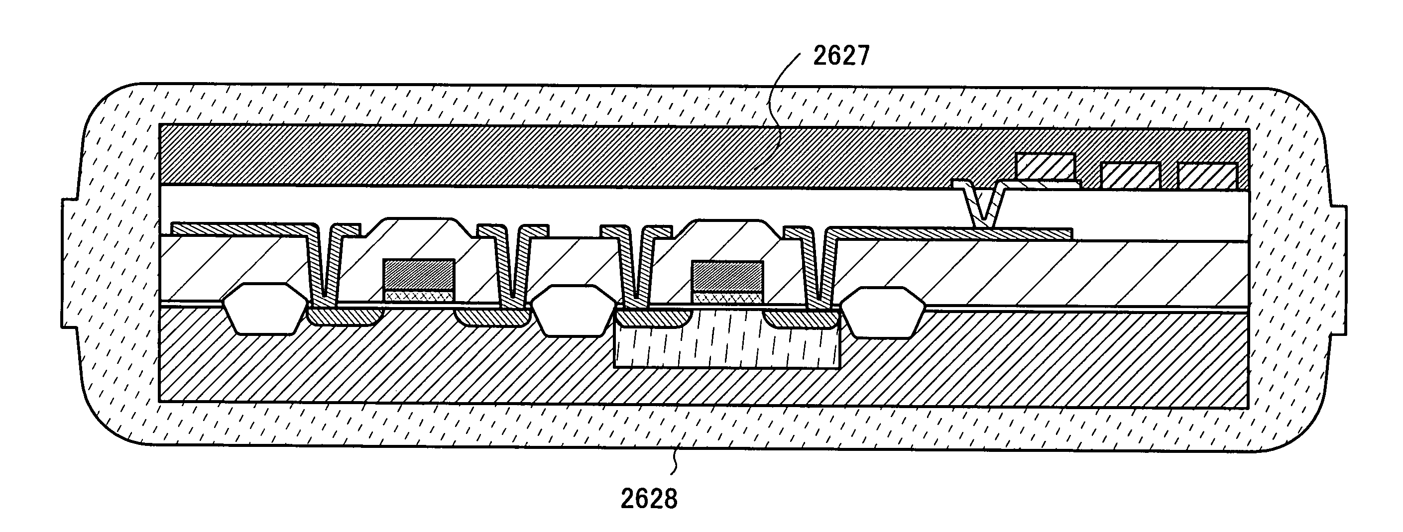
[0078]In this embodiment mode, an example of fabricating a transistor included in the semiconductor device described in any of the above embodiment modes is described. In this embodiment mode, a mode is particularly described in which a semiconductor device provided with a transistor fabricated using a semiconductor film formed over an insulating substrate is formed.

[0079]First, a release layer 1902 is formed on one surface of a substrate 1901, and then an insulating film 1903 to be a base and an amorphous semiconductor film 1904 (for example, a film containing amorphous silicon) are formed (FIG. 9A). The release layer 1902, the insulating film 1903, and the amorphous semiconductor film 1904 can be successively formed. Being formed successively, they are not exposed to the air and thus mixture of an impurity can be prevented.

[0080]As the substrate 1901, a glass substrate, a quartz substrate, a metal substrate, a stainless steel substrate, a plastic substrate which has heat resistanc...


PUM


Abstract

A charge accumulation circuit having a structure in which a capacitor is divided into a plurality of pieces and the divided capacitors are connected in parallel through switches is provided. The charge accumulation circuit controls the switch provided between the capacitors and thus can dynamically vary electrostatic capacitance of the charge accumulation circuit which applies a voltage to a constant voltage circuit.

Description

BACKGROUND OF THE INVENTION[0001]1. Field of the Invention[0002]The present invention relates to a semiconductor device. The present invention particularly relates to a semiconductor device capable of wirelessly communicating data, a so-called IC chip (also referred to as an ID chip or a transponder) for RFID (radio frequency identification).[0003]Note that a semiconductor device described in this description refers to a general device capable of functioning by utilizing semiconductor characteristics.[0004]2. Description of the Related Art[0005]In recent years, it is called ubiquitous information society that an environment in which it is possible to access an information network anytime and anywhere has been put into place. In such environment, an individual identification technique in which an ID (individual identification number) is given to an individual object to clarify records of the object so that it is useful for production, management, and the like has been researched for ...

Claims


Application Information

Patent Timeline
Patent Type & Authority Patents(United States)
IPC IPC(8): H04Q5/22
CPCG06K19/0701G06K19/0723H01Q1/2225H01Q1/248H02M3/07
Inventor KAWAE, DAISUKEIKEDA, TAKAYUKIKOZUMA, MUNEHIRO
Owner SEMICON ENERGY LAB CO LTD
Why Eureka
Try Eureka