Nonvolatile storage device and method for manufacturing the same in which insulating film is located between first and second impurity diffusion regions but absent on first impurity diffusion region

a technology of nonvolatile storage and manufacturing method, which is applied in the direction of semiconductor devices, basic electric elements, electrical apparatus, etc., can solve the problems of disadvantageous miniaturization, and achieve the advantages of miniaturization, less variation in initial threshold value, and excellent trap memory

Active Publication Date: 2013-01-01
NEC CORP
View PDF21 Cites 7 Cited by
  • Summary
  • Abstract
  • Description
  • Claims
  • Application Information

AI Technical Summary

Benefits of technology

[0019]FIG. 32 is an enlarged view showing a region around drain region 6 of the second conventional structure. The second conventional structure has a charge accumulating region expanding even outwardly of gate sidewall portion 16 and, for this reason, the writing efficiency of accumulated charge is improved as compared with the first conventional structure. Further, since edge portions of the insulating films are not damaged by dry etching, an improvement can be made in lessening leakage of accumulated charge toward the substrate and the electrode.
[0059]By using the nonvolatile storage device and the manufacturing method thereof according to the present invention, it is possible to form excellent trap type memory which is advantageous in miniaturization and subject to less variation in initial threshold value, exhibits a high writing efficiency and is free from an erasing failure and a retention failure.

Problems solved by technology

However, even when the second conventional structure thus improved and its manufacturing method are used, the following problems arise.
(1) Expanding the charge accumulating layer up to the outside of gate sidewall 16 is disadvantageous in miniaturization.

Method used


Image

  • Nonvolatile storage device and method for manufacturing the same in which insulating film is located between first and second impurity diffusion regions but absent on first impurity diffusion region
  • Nonvolatile storage device and method for manufacturing the same in which insulating film is located between first and second impurity diffusion regions but absent on first impurity diffusion region
  • Nonvolatile storage device and method for manufacturing the same in which insulating film is located between first and second impurity diffusion regions but absent on first impurity diffusion region

Examples


first exemplary embodiment

Nonvolatile Storage Device

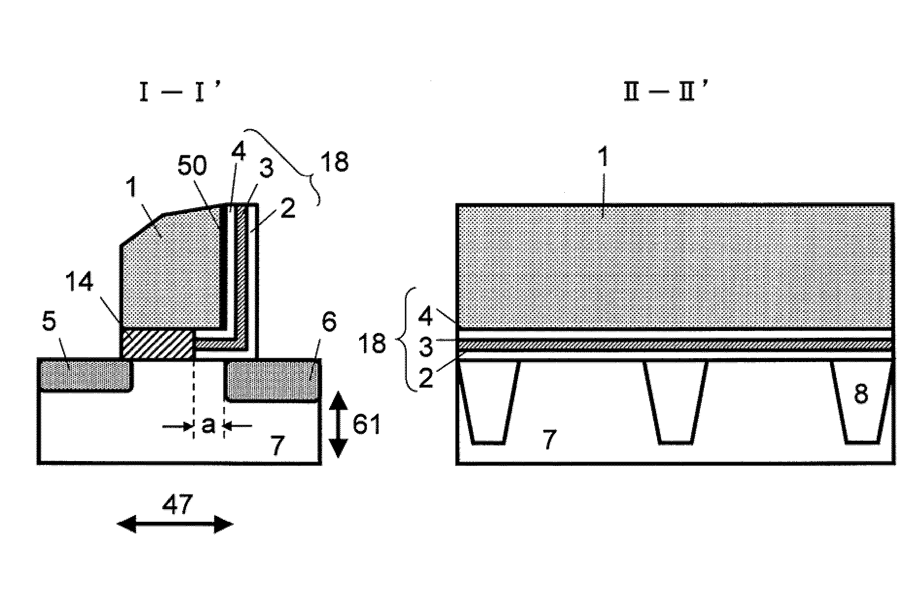
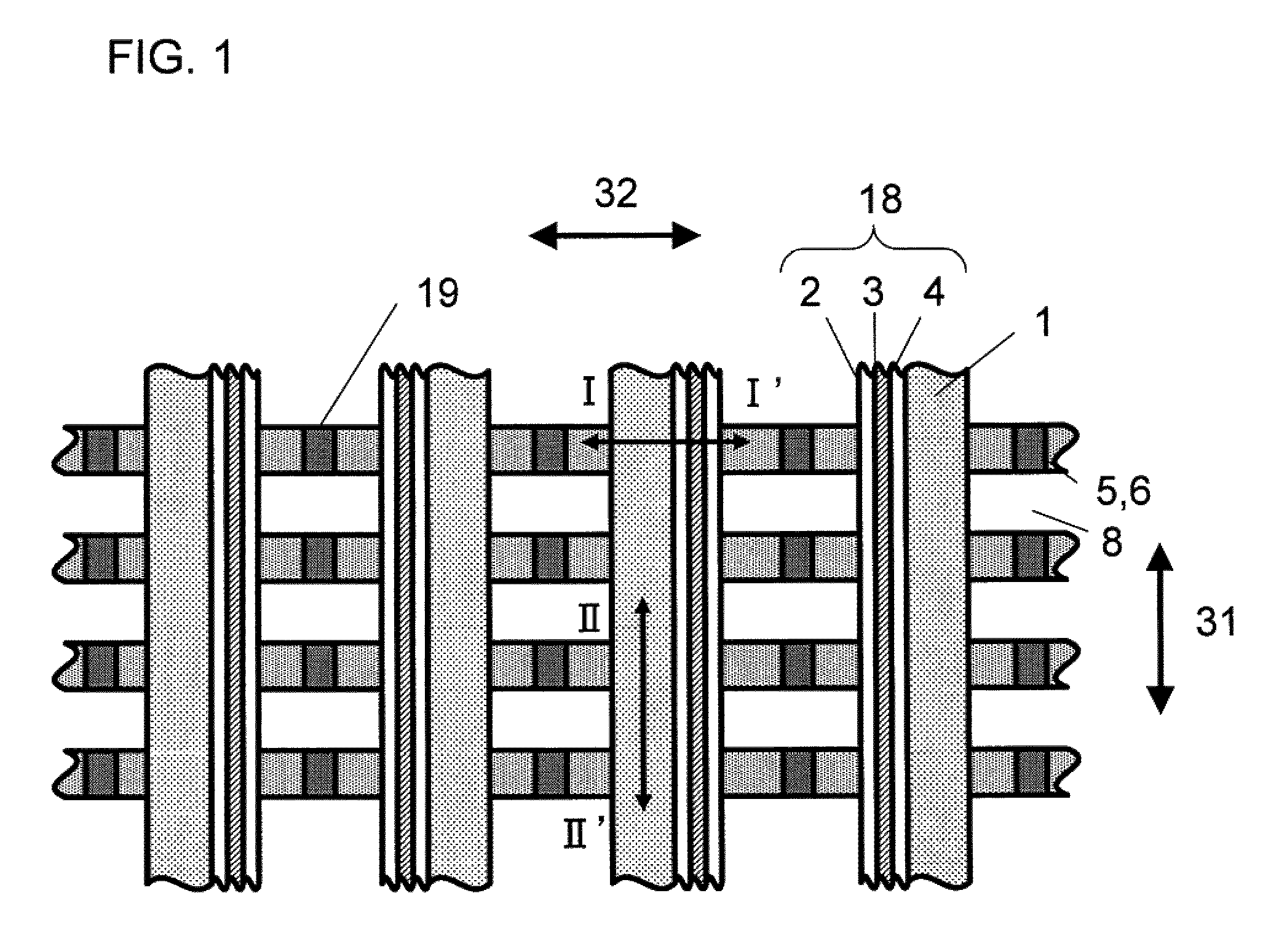
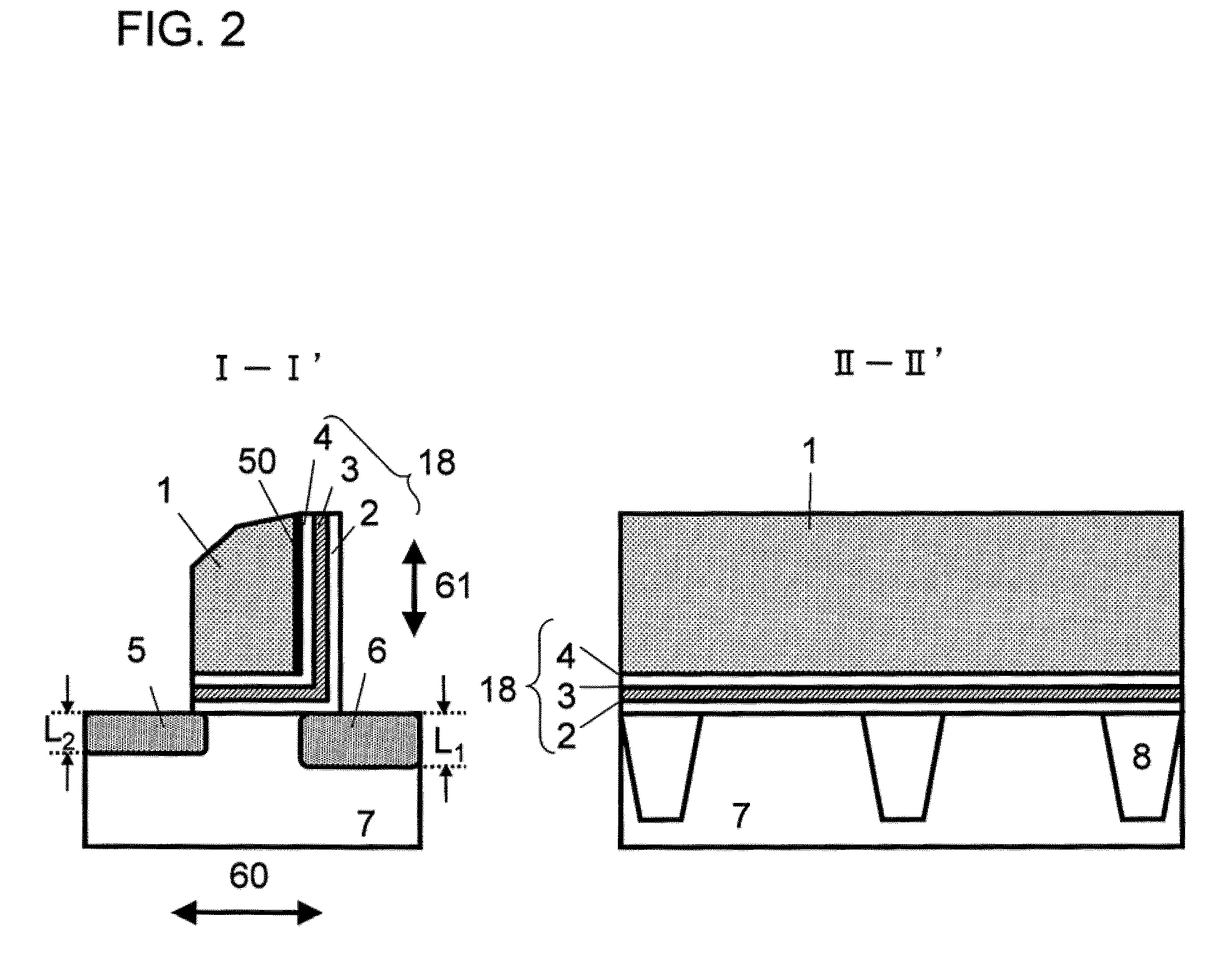
[0166]FIGS. 5 and 6 illustrate trap type memory (i.e., nonvolatile storage device) according to a first exemplary embodiment. FIG. 5 is a top view of the nonvolatile storage device, and FIG. 6 includes sectional views taken along line I-I′ and line II-II′ of FIG. 5.

[0167]As shown in FIGS. 5 and 6, a plurality of line electrodes extending in predetermined direction 31 are provided on silicon substrate 7 provided with isolation regions 8. Drain region 6 and source region 5 which is present in a shallower region than drain region 6 are provided in silicon substrate 7 so as to be opposed to each other in direction 32 perpendicular to direction 31 in which the line electrodes extend. Drain region 6 and source region 5 are formed so as to partially overlap film stack 18 (i.e., such that drain region 6 and source region 5 is partially in contact with film stack 18). In this exemplary embodiments drain region 6 and source region 5 are defined as the first impurity ...

second exemplary embodiment

Nonvolatile Storage Device

[0195]FIGS. 8 and 9 illustrate trap type memory (i.e., nonvolatile storage device) according to a second exemplary embodiment. FIG. 8 is a top view of the trap type memory according to the second exemplary embodiment, and FIG. 9 illustrates sectional views of the trap type memory according to the present exemplary embodiment taken along line I-I′ and line II-II′ of FIG. 8.

[0196]As shown in FIGS. 8 and 9, a plurality of line electrodes extending in predetermined direction 31 are provided on silicon substrate 7 provided with isolation regions 8. Each of the line electrodes includes two side surfaces extending vertically to the plane direction of semiconductor substrate 7. Film stack (i.e., stacked films) 18 is provided which extends from between the line electrode and the semiconductor substrate onto one side surface (i.e., the surface lying on the first impurity diffusion region side) of the line electrode extending vertically to the plane direction of the s...

third exemplary embodiment

Nonvolatile Storage Device

[0216]FIGS. 11 and 12 illustrate trap type memory (i.e., nonvolatile storage device) according to a third exemplary embodiment. FIG. 11 is a top view of the trap type memory according to the third exemplary embodiment, and FIG. 12 illustrates sectional views of the trap type memory according to the present invention taken along line I-I′ and line II-II′ of FIG. 12.

[0217]As shown in FIGS. 11 and 12, a pair of two line electrodes extending in predetermined direction 31 are provided on silicon substrate 7 provided with isolation regions 8. Such a plurality of pairs of line electrodes are provided on the semiconductor substrate. Drain region (i.e., impurity diffusion region B) 6, diffusion layer (i.e., impurity diffusion region A) 13 and source region (i.e., impurity diffusion region C) 5 are provided in silicon substrate 7 in a line and arranged as opposed to each other in direction 32 perpendicular to direction 31 in which the line electrodes extend. Diffusio...


PUM


Abstract

Provided is an excellent nonvolatile storage device having advantageous in miniaturization and less variation in initial threshold value, and exhibiting a high writing efficiency, without an erasing failure and a retention failure. The nonvolatile storage device is characterized by including a film stack extending from between a semiconductor substrate and a gate electrode onto at least a surface of the gate electrode lying on a first impurity diffusion region side, the film stack including a charge accumulating layer and a tunnel insulating film sequentially from a gate electrode side.

Description

[0001]This application is the National Phase of PCT / JP2007 / 074024, filed Dec. 13, 2007, which is based upon and claims the benefit of priority from Japanese Patent Application No. 2006-338196, filed on Dec. 15, 2006, the disclosure of which is incorporated herein in its entirety by reference.TECHNICAL FIELD[0002]The present invention relates to a nonvolatile storage device and a method for manufacturing the same.BACKGROUND ART[0003]In recent years, development has been actively made of a nonvolatile storage device which does not allow data stored therein to disappear even when an external power source is turned OFF. Reduction in cell area using Floating Gate (FG) type memory and thinning of an insulating film have been the main stream of FLASH memory miniaturization up to the 0.13-μm generation. With respect to the 90-nm generation and later, however, the thinning of an insulating film has become difficult from the viewpoint of data retention properties securing and, hence, attentio...

Claims


Application Information

Patent Timeline
Patent Type & Authority Patents(United States)
IPC IPC(8): H01L29/792
CPCH01L21/28282H01L27/11568H01L29/401H01L29/66833H01L29/792H01L29/4234H01L29/40117H01L29/40114H10B43/30
Inventor TSUJI, YUKIHIDE
Owner NEC CORP
Why Eureka
Try Eureka