
System and method for adaptive timing control of successive approximation analog-to-digital conversion

a technology of successive approximation and adaptive timing control, applied in the field of system and method for timing generation in successive approximation register (sar) analog-to-digital conversion, can solve the problems of insufficient allocation of available sar processing cycle time, and failure of optimization timing to ensure adequate tim

Active Publication Date: 2013-01-01
CADENCE DESIGN SYST INC
View PDF12 Cites 54 Cited by
  • Summary
  • Abstract
  • Description
  • Claims
  • Application Information

AI Technical Summary

Benefits of technology

The present invention relates to a system and method that automatically generates timing for the execution of SAR ADC processing cycles, ensures that enough time is allocated between the sampling and bit conversion phases, and enables selectivity over the generated timing. These features allow for efficient and effective execution of SAR ADC processing.

Problems solved by technology

For deep submicron semiconductor technologies, for instance, it is a significant challenge to preserve ample timing for full and proper execution of SAR ADC processing cycles.
While such approaches do improve timing efficiencies, they do not ensure ample allocation of the available SAR processing cycle time between the sampling and conversion phases (successive bit determinations) of each cycle.
The known attempts to optimize timing fail to ensure adequate time for settling of the internal reference DAC between successive bit determinations.

Method used


Image

  • System and method for adaptive timing control of successive approximation analog-to-digital conversion
  • System and method for adaptive timing control of successive approximation analog-to-digital conversion
  • System and method for adaptive timing control of successive approximation analog-to-digital conversion

Examples


Embodiment Construction

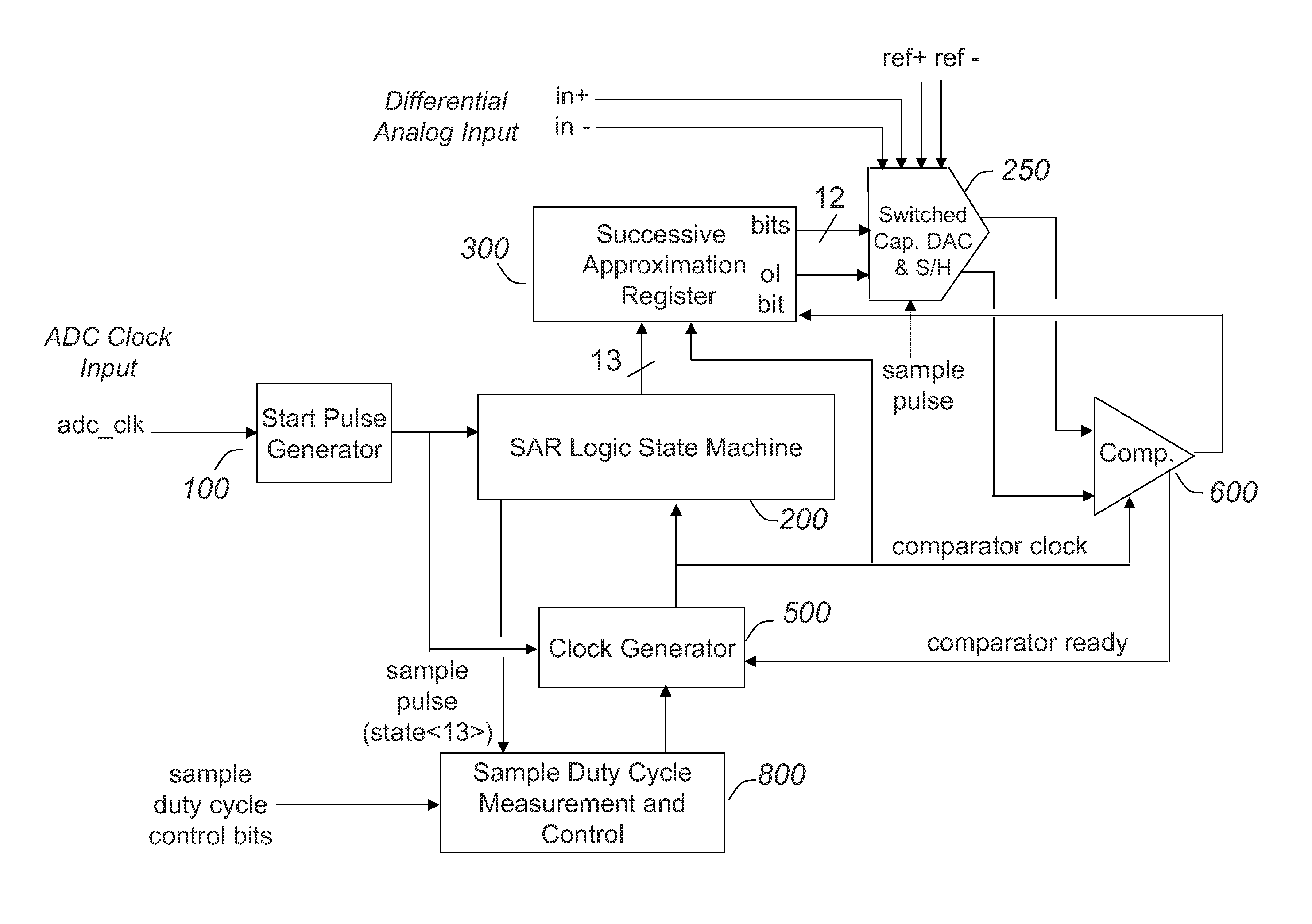
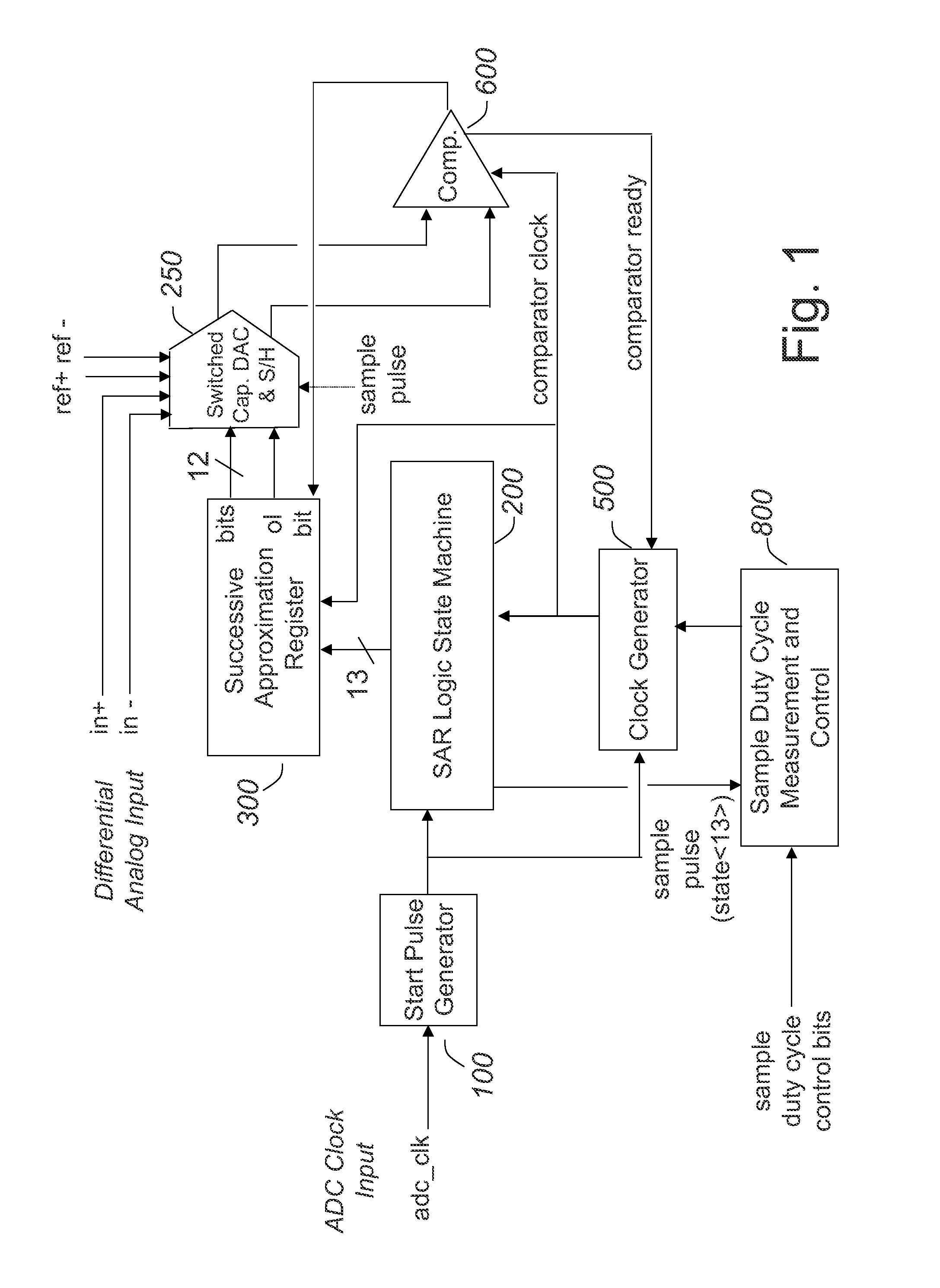
[0024]Referring now to FIG. 1, there is shown a system 10 formed in accordance with an exemplary embodiment of the present invention. System 10 generally provides a successive approximation register (SAR) analog-to-digital converter (ADC) with adaptive timing generation. SAR ADC processing is effectively carried out by a system 10 which includes a SAR logic state machine unit 200, successive approximation register (SA Register) unit 300, reference digital-to-analog DAC converter & sample / hold (S / H) unit 250, and comparator unit 600 preferably inter-coupled as shown. Although separately shown, the successive approximation register of unit 300 may be formed as part of SAR logic state machine unit 200.

Timed SAR ADC

[0025]As mentioned, an SAR ADC processing cycle includes a sampling phase followed by a bit conversion phase. During the sampling phase, reference DAC & S / H unit 250 samples and holds (for the subsequent bit conversion phase) an analog input voltage VIN, which in the illustra...


PUM


Abstract

A system and method are provided for adaptively controlling timing in SAR ADC of a sampled analog signal within a conversion period. A state machine maintains a set of SAR states including a sampling state and a plurality of bit conversion states. A reference generator generates a quantization level reference for each of the bit conversion states within a parametric settling time thereof. A comparator compares the sampled analog signal with the quantization level reference over a parametric propagation time for determining a hit value for each hit conversion state. A clock generator adaptively defines signals for clocking the state machine and comparator for each SAR state, thereby adaptively delaying bit determination in each bit conversion state by an integration period not less than the settling time, while adaptively delaying quantization level reference generation for a next bit conversion state by a regeneration period not less than the propagation time.

Description

BACKGROUND OF THE INVENTION[0001]The present invention is generally directed to a system and method for timing generation in successive approximation register (SAR) analog-to-digital conversion. More specifically, the subject system and method provide for selective generation of a timing profile used in actuating an SAR analog-to-digital converter ADC.[0002]SAR ADC architecture has long been favored in many applications requiring high speed, low power consumption, and suitably high conversion resolution. For conversion to an n-bit digital word, an SAR ADC generally operates to sample an analog input signal voltage then carry out a binary search for the corresponding quantized level to be coded via the n-hit word. The binary search is carried out over each of the bit positions in the n-bit word, with a comparator comparing the sampled input signal voltage against a succession of voltage reference levels. This comparison is thereby made for each successive “state” of the n-bit word as...

Claims


Application Information

Patent Timeline
IPC IPC(8): H03M1/12
CPCH03M1/462
Inventor EVANS, WILLIAM PIERCE
Owner CADENCE DESIGN SYST INC
Learn More