Programmable resistance memory

a technology of programmable resistance and memory, applied in the field of electronic memory devices, can solve the problems of increasing the complexity of the peripheral circuitry that supports the memory array, the process of producing a given circuit in cmos technology, and the implementation of a comparable circuit. achieve the effect of simplifying circuit design, reducing supply voltage, and reducing static power consumption

Active Publication Date: 2013-01-08
OVONYX MEMORY TECH LLC
View PDF11 Cites 24 Cited by
  • Summary
  • Abstract
  • Description
  • Claims
  • Application Information

AI Technical Summary

Benefits of technology

[0013]Unipolar MOS technologies (that is, NMOS and PMOS technologies) antedate the CMOS technology which has substantially supplanted the older unipolar MOS and bipolar technologies in commercial integrated circuit production. As is known in the art, circuits based on CMOS technology typically boast considerably lower static power consumption than circuits based on either PMOS or NMOS technology. Digital circuits based on CMOS technology also produce output swings that encompass the entire range of a circuit's supply voltage. The availability of complementary transistors in CMOS technology greatly simplifies circuit design, when compared to the design of circuits of similar function implemented in non-CMOS technology. Additionally, CMOS does not require boot strapped gates and can generally operate at lower supply voltages than other technologies. For these reasons, CMOS technology has become the technology of choice in digital logic and memory applications. However, the process of producing a given circuit in CMOS technology is substantially more complex than a comparable circuit implemented in unipolar MOS technologies.
[0014]Rather than focusing exclusively on programmable resistance memory cells and related technologies to reduce the cost of production, the applicant has devised a programmable resistance memory device and process architecture that greatly simplifies the production of the peripheral circuitry that supports a programmable resistance memory. In this way, a programmable resistance memory in accordance with the principles of the present invention may be produced at a substantially lower cost than conventional programmable resistance memories. In particular, as memory devices steadily increase in capacity, the peripheral circuitry that supports the memory array becomes more and more complex. In order to accommodate that complexity, additional process steps must be included to incorporate the additional layers of interconnect needed to define the increasingly complex support circuits. This is particularly true of CMOS circuitry because considerable additional processing is required to build 2 types of MOS transistors; N-ch and P-ch MOSFETS. By employing unipolar MOS peripheral circuitry in accordance with the principles of the present invention, a programmable resistance memory in accordance with the principles of the present invention may be produced using a much simpler production process than that required for a programmable resistance memory of comparable capacity employing CMOS peripheral circuitry. In an illustrative method in accordance with the principles of the present invention, a unipolar MOS programmable resistance memory may be produced with fewer than eleven mask steps, no more than five of which are critical mask steps. Recognizing that phase change memories do not require the full supply-voltage logic swings provided by CMOS technology, that the power dissipation of unipolar MOS circuits may be brought in line with CMOS technology by, for example, turning unipolar devices off whenever the memory is not being accessed, and that the higher design costs associated with unipolar MOS design may be amortized over a large number of unipolar MOS phase change memory devices that may be produced much more efficiently than CMOS phase change memory devices, a programmable resistance memory in accordance with the principles of the present invention employs unipolar MOS, rather than CMOS technology, for the memory's peripheral circuitry.
[0015]Additional cost reductions may be achieved in accordance with the principles of the present invention by reducing the extent of unipolar peripheral circuitry included on each standalone memory. Such a reduction in circuitry increases the number of standalone memory devices that may be produced from a given wafer and, at the same time, increases the yield of devices produced. As an added benefit, by offloading the functionality of a portion of the peripheral circuitry, a programmable resistance memory in accordance with the principles of the present invention reduces its power consumption.
[0016]In an illustrative system embodiment, the functionality of the offloaded peripheral circuitry is incorporated in a peripheral circuit device, such as a memory controller, that may be implemented in a lower-power technology, such as CMOS, for example. The offloaded functionality from a plurality of unipolar MOS programmable resistance memories in accordance with the principles of the present invention may be consolidated in such a peripheral circuit device. In this manner, a programmable resistance memory system in accordance with the principles of the present invention may reap the substantial cost benefits of low-complexity, low-mask-step programmable resistance memory devices while, at the same time, reducing die size and paying little or no power penalty in comparison with conventional programmable resistance memories that employ on-chip CMOS peripheral circuitry.
[0018]In an illustrative, minimal-configuration embodiment, a programmable resistance memory in accordance with the principles of the present invention includes only a programmable resistance array, unipolar row and column drivers, unipolar address decoder circuitry, and unipolar I / O circuitry; all other peripheral circuitry is offloaded to one or more other integrated circuits. A programmable resistance memory in accordance with the principles of the present invention may employ epitaxial diodes as isolation devices within the devices' memory array. Epitaxial diodes provide superior operating characteristics and their production process permits the use of low-resistivity conductors, such as copper, for example, to interconnect a memory's various devices. Copper interconnection provides higher conductivity and is less susceptible to electro-migration failure than conventional, aluminum or tungsten, interconnection. In accordance with the principles of the present invention, the copper interconnection may be used to “strap,” or “mirror,” drive circuits within a memory's substrate, thereby drastically reducing the resistance within a memory's signal path and providing higher signal margins. In an illustrative embodiment an N+ region within a substrate is used as a local rowline to which epitaxial cathodes are connected. A strapping connection is made between the local N+ rowline and a copper interconnect line spaced every thirty-two memory elements. In another illustrative embodiment, the connection is made at least every sixteen memory elements. To reduce resistance in the rowline even further a strapping connection may be made every eight memory elements of a rowline.

Problems solved by technology

However, the process of producing a given circuit in CMOS technology is substantially more complex than a comparable circuit implemented in unipolar MOS technologies.
In particular, as memory devices steadily increase in capacity, the peripheral circuitry that supports the memory array becomes more and more complex.

Method used


Image

  • Programmable resistance memory
  • Programmable resistance memory
  • Programmable resistance memory

Examples


Embodiment Construction

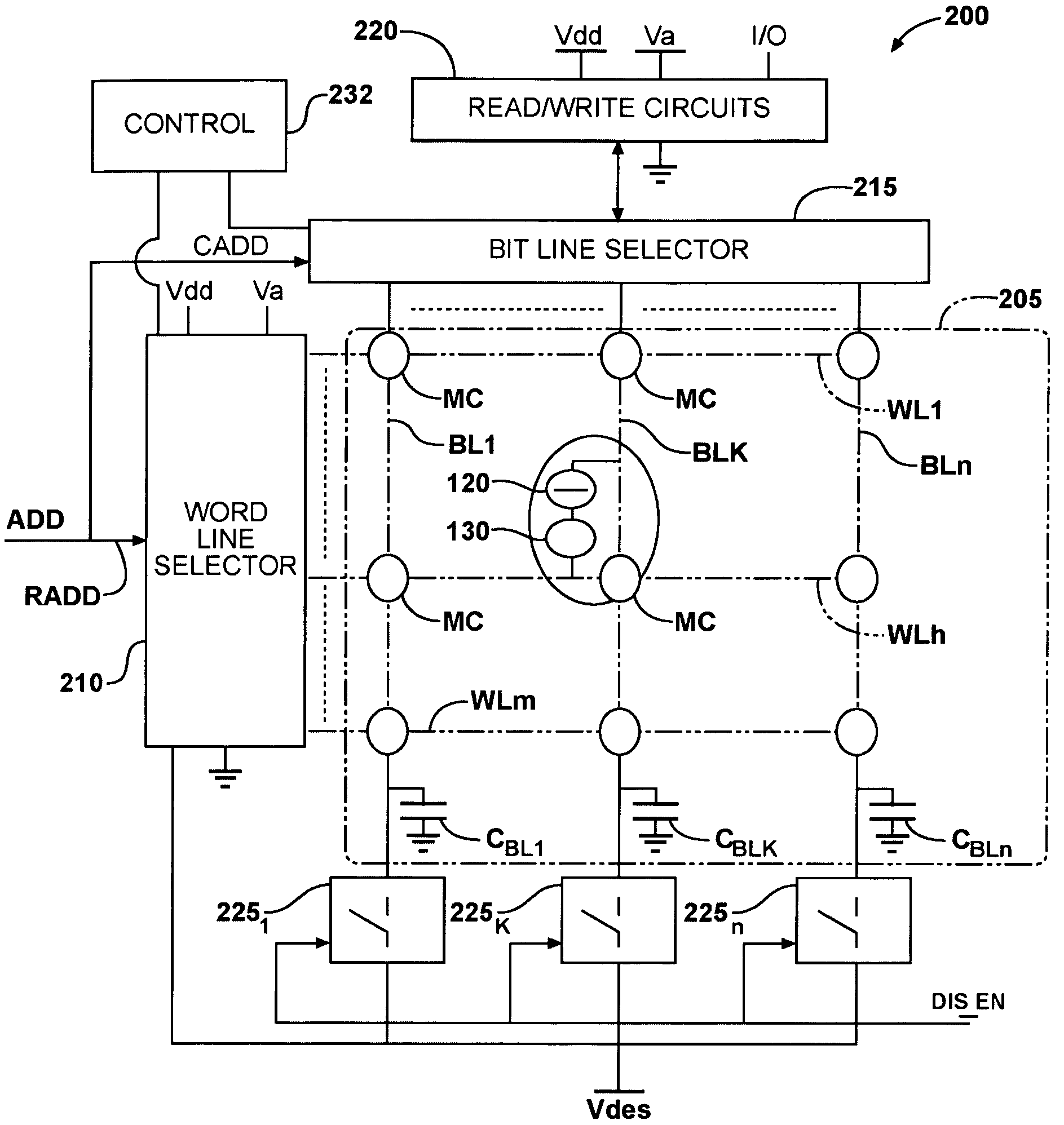
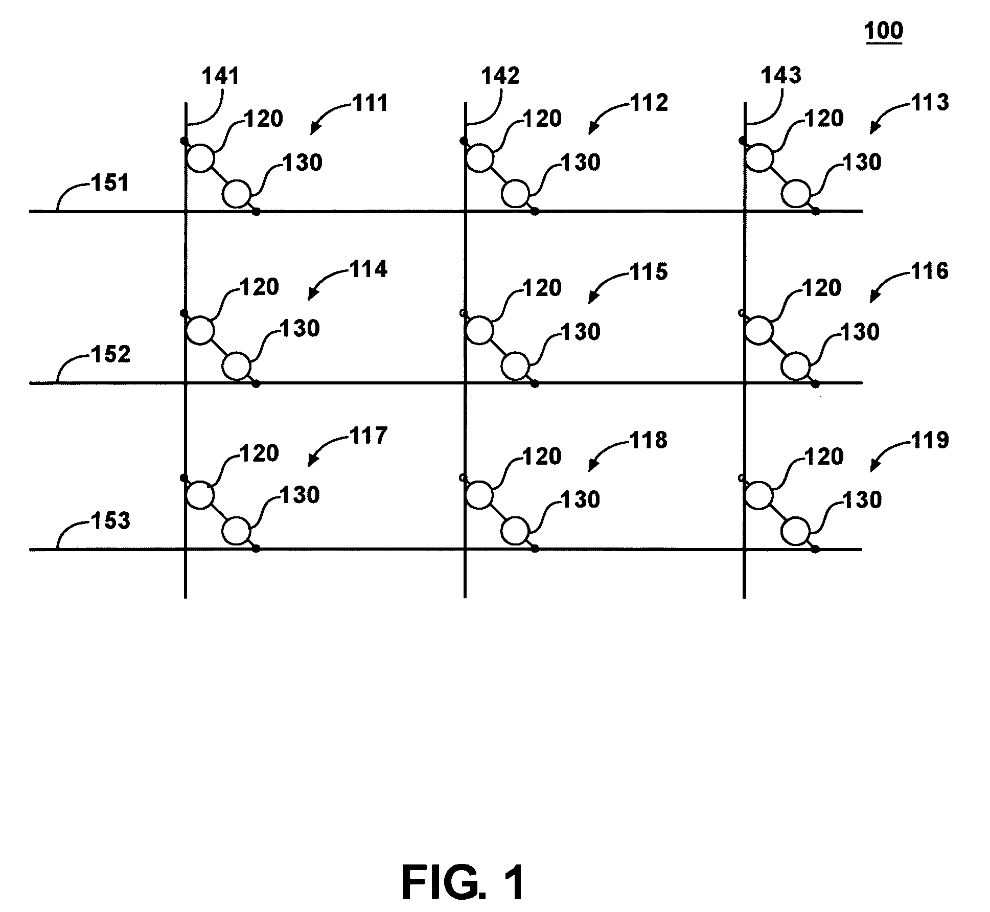
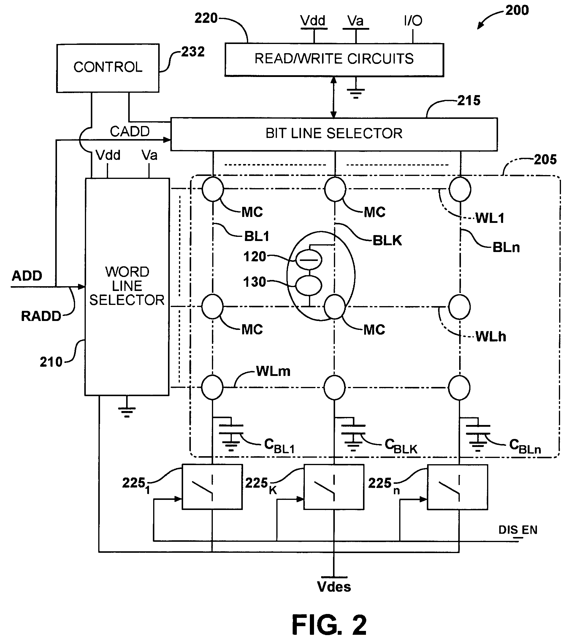
[0030]Although this invention will be described in terms of certain preferred embodiments, other embodiments that are apparent to those of ordinary skill in the art, including embodiments that do not provide all of the benefits and features set forth herein, are also within the scope of this invention. Various structural, logical, process step, chemical, and electrical changes may be made without departing from the spirit or scope of the invention. Polarities and types of devices and supplies may be substituted in a manner that would be apparent to one of reasonable skill in the art. Process descriptions may include flowcharts that illustrate various steps taken in a process. Such flowcharts and accompanying discussion are not meant to be an exhaustive explanation of every step and every procedure in such a process. Rather, they are meant to provide a description with sufficient detail to enable one of ordinary skill in the art to practice and use the invention. In some embodiments,...


PUM


Abstract

A memory includes a programmable resistance array and unipolar MOS peripheral circuitry. The peripheral circuitry includes address decoding circuitry. Because unipolar MOS circuitry is employed, the number of mask steps and, concomitantly, the cost of the programmable resistance memory may be minimized.

Description

CROSS-REFERENCE TO RELATED APPLICATIONS[0001]1. Field of Invention[0002]This invention relates to electronic memory devices.[0003]2. Background of the Invention[0004]As electronic memories approach limits beyond which they will no longer be able to produce the density / cost / performance improvements so famously set forth in Moore's law, a host of memory technologies are being investigated as potential replacements for conventional silicon complementary metal oxide semiconductor (CMOS) integrated circuit memories. Among the technologies being investigated are programmable resistance technologies, such as phase change memory technologies. Phase-change memory arrays are based upon memory elements that switch among two material phases, or gradations thereof, to exhibit corresponding distinct electrical characteristics. Alloys of elements of group VI of the periodic table, such as Te, S or Se, referred to as chalcogenides or chalcogenic materials, can be used advantageously in phase change...

Claims


Application Information

Patent Timeline
Patent Type & Authority Patents(United States)
IPC IPC(8): G11C11/00
CPCG11C13/0004G11C2213/72
Inventor LOWREY, TYLER
Owner OVONYX MEMORY TECH LLC
Why Eureka
Try Eureka