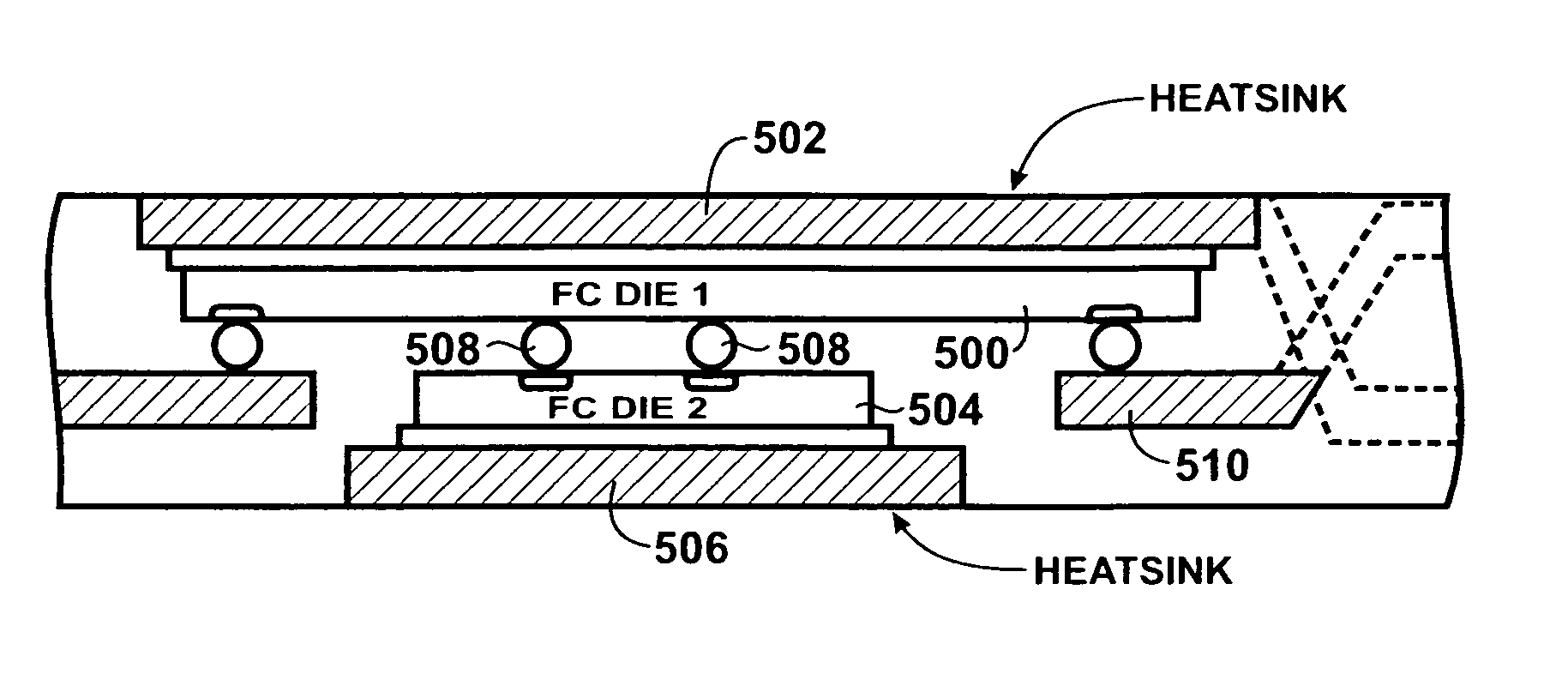
Semiconductor package featuring flip-chip die sandwiched between metal layers
a technology of metal layers and semiconductors, applied in the direction of semiconductor devices, semiconductor/solid-state device details, electrical apparatus, etc., can solve the problems of expensive wire bonding steps, difficult wire bonding steps, and inability to perform wire bonding, so as to avoid the expense of wire bonding and improve heat dissipation.
- Summary
- Abstract
- Description
- Claims
- Application Information
AI Technical Summary
Benefits of technology
Problems solved by technology
Method used
Image


Examples
Embodiment Construction
[0039]FIG. 2 is a simplified plan view of an embodiment of a package in accordance with the present invention. FIG. 2A is a simplified cross-sectional view of the package of FIG. 2, taken along the cross-sectional line 2A-2A′.
[0040]Package 200 comprises MOSFET die 202 having a top surface featuring gate pad 204 and source pad 206. The bottom surface of MOSFET die 202 features a drain contact 208.
[0041]Drain contact 208 is in electrical communication with an underlying first metal layer 224, through electrically and thermally conducting adhesive material 220. One example of such an electrically and thermally conducting material is solder. In certain embodiments, the first metal layer can be provided pre-bumped with solder balls or pre-formed with a solderable contact surface.
[0042]Integral projections of the first metal layer 224 extend outside of the plastic package body to provide leads for electrical contact with the MOSFET drain. The underside portion of the first metal layer tha...
PUM
 Abstract
Description
Claims
Application Information