Electronic control device

a control device and electronic technology, applied in the direction of electrical apparatus casings/cabinets/drawers, electrical apparatus details, etc., can solve the problems of increasing the number of wiring harnesses, increasing the stress of different amounts, and increasing the difficulty of securing a space for mounting various devices, so as to prevent interfacial peeling, reduce stress, and secure radiation performance

Active Publication Date: 2013-01-22
DENSO CORP
View PDF16 Cites 6 Cited by
  • Summary
  • Abstract
  • Description
  • Claims
  • Application Information

AI Technical Summary

Benefits of technology

[0018]In view of the above points, it is an object of the present invention to provide an electronic control device that has a half mold structure in order to secure radiation performance, and that can prevent interfacial peeling between an edge portion of a circuit board and a molding resin.
[0019]According to one aspect of the present invention, an electronic control device includes a circuit board having a first surface and a second surface that is an opposite surface of the first surface, a base member configured to be used as a heat sink, an electronic component mounted on the first surface, a molding resin sealing at least the circuit board and a surface of the base member to which the circuit board is attached, and a stress reducing portion arranged at least on an outer edge portion of the first surface of the circuit board. The base member is bonded to the second surface. The stress reducing portion is configured such that stress of a joint portion between the circuit board and the molding resin via the stress reducing portion at the outer edge portion is lower than stress of a joint portion between the circuit board and the molding resin which are directly bonded to each other. An elastic modulus of the stress reducing portion is lower than an elastic modulus of the circuit board.
[0020]In the above configuration, the elastic modulus of the stress reducing portion is lower than the elastic modulus of the circuit board, that is, the stress reducing portion is softer than the circuit board. The stress reducing portion is more likely to deform than the circuit board and can reduce stress received from the molding resin. Therefore, even when peeling stress is applied to an interface between the outer edge portion of the first surface of the circuit board and the molding resin, the peeling stress can be reduced by the stress reducing portion.
[0021]The peeling stress in the molding resin is generated from an outer edge portion of the circuit board toward the center thereof. Thus, interfacial peeling at the outer edge portion of the first surface of the circuit board, at which the peeling stress is most likely to be generated in the circuit board, can be prevented.
[0022]Therefore, the interfacial peeling between the outer edge portion of the first surface of the circuit board and the molding resin can be prevented.
[0023]Further, the electronic control device has a half mold structure, and thereby radiation performance of the electronic component can be improved.

Problems solved by technology

Furthermore, as the number of electronic control devices is increased, the number of wiring harnesses may be increased and securing a space for mounting various devices becomes difficult.
However, in a large-size component such as a control circuit for a transmission, stress due to the difference between the amount of heat contraction of a molding resin and components such as a circuit board and a base member is so large that peeling at an interface may be generated.
Thus, heat generated at the electronic components is released to outside through the flange portion arranged at the base member and exposed to outside from the molding resin, so that radiation performance may be decreased.
That is, even if the molding resin contracts at one surface of the base member, because the molding resin is not arranged on another surface thereof, it becomes difficult to maintain balance of contraction in the molded device.
Thus, it is difficult to prevent the warpage of the molded device as a whole, and reliability in adhesion at an interface of the molding resin may be decreased.
In both structures described in JP-A-2004-119465 and JP-A-2008-084978, the linear expansion coefficients of the molding resin and the base member can be set to be about 8 to 10 ppm / ° C. However, a linear expansion coefficient of ceramic used for the circuit board is about 5 to 7 ppm / ° C., and it is difficult for the linear expansion coefficients of the molding resin and the base member to set to be approximately equal to that of the circuit board.
However, because a viscosity of the adhesion improving member is low such that the circuit board is uniformly coated with the adhesion improving member by spraying, a thickness of the adhesion improving member at a flat portion such as the edge portion may become small.
Although adhesion between the molding resin and the circuit board can be improved, there is a limit to reduce the stress due to the low elasticity.
Therefore, even when the base member is made of the same material with the molding resin and the adhesion between the molding resin and the circuit board is improved, interfacial peeling at the edge portion of the circuit board cannot be prevented.
Thus, a bonding wire of the electronic component mounted on the circuit board may be cut, for example, so that electronic failure may generate.

Method used


Image

  • Electronic control device
  • Electronic control device
  • Electronic control device

Examples


first embodiment

[0047]Hereinafter, a first embodiment of the present invention will be described with reference to FIGS. 1 to 6. An electronic control device according to the present embodiment is used as an in-vehicle electronic control device, for example. Specifically, the electronic control device is used as an electronic control device for an automatic transmission, and is equipped in a valve body arranged inside the automatic transmission as a module integrated with a solenoid, various sensors and the like.

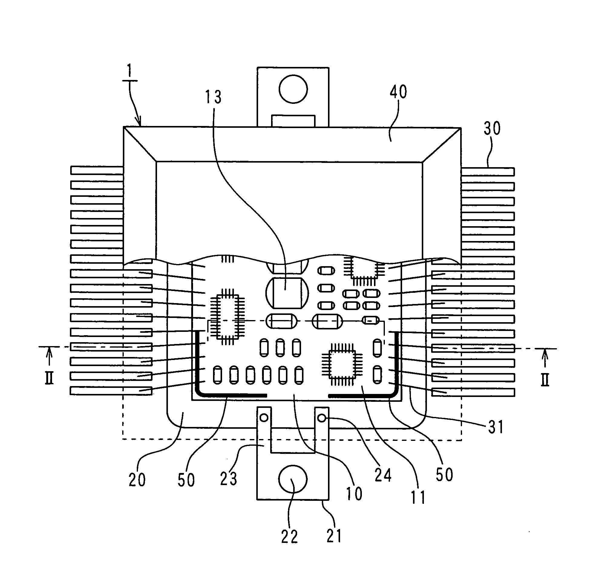
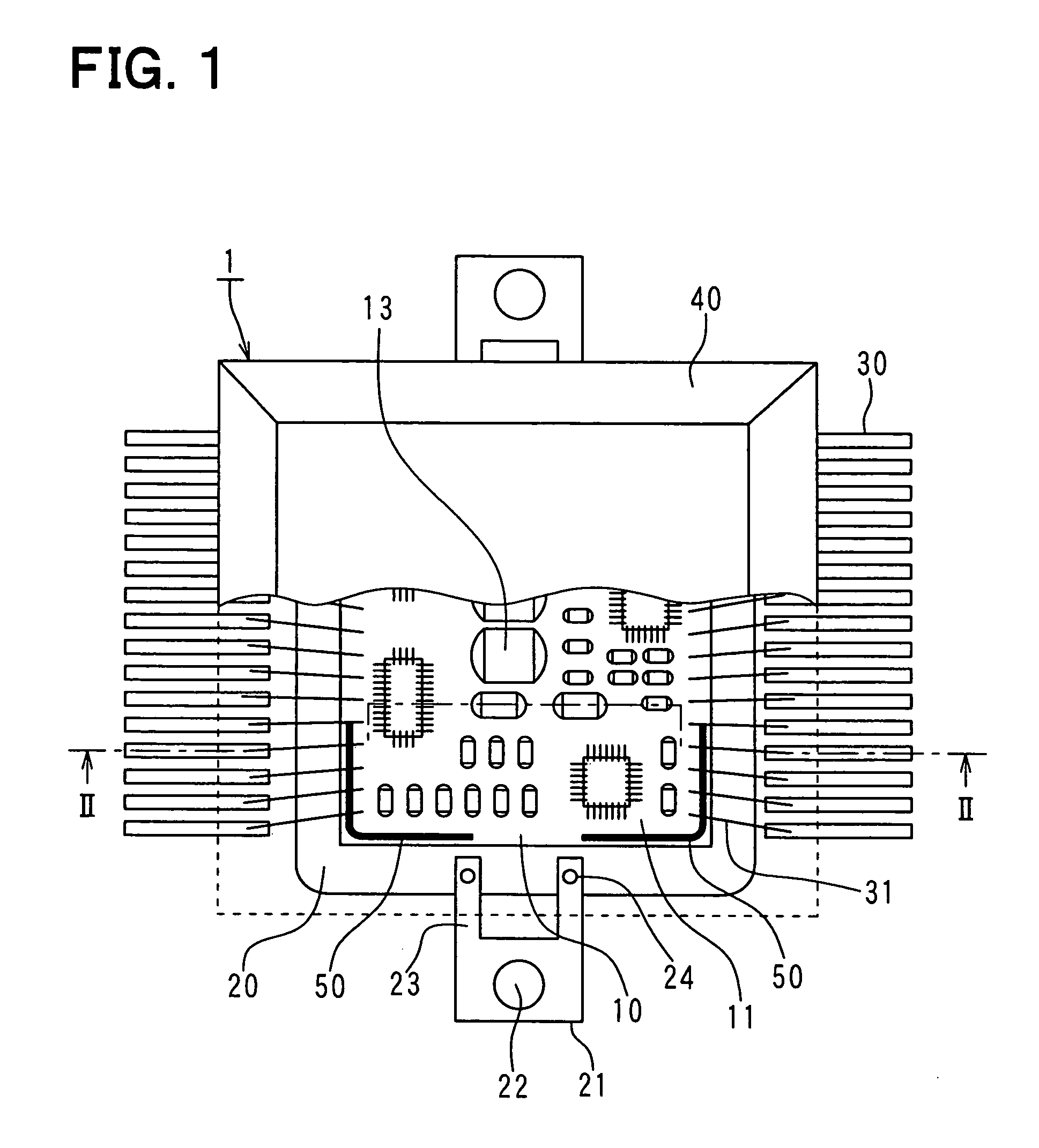
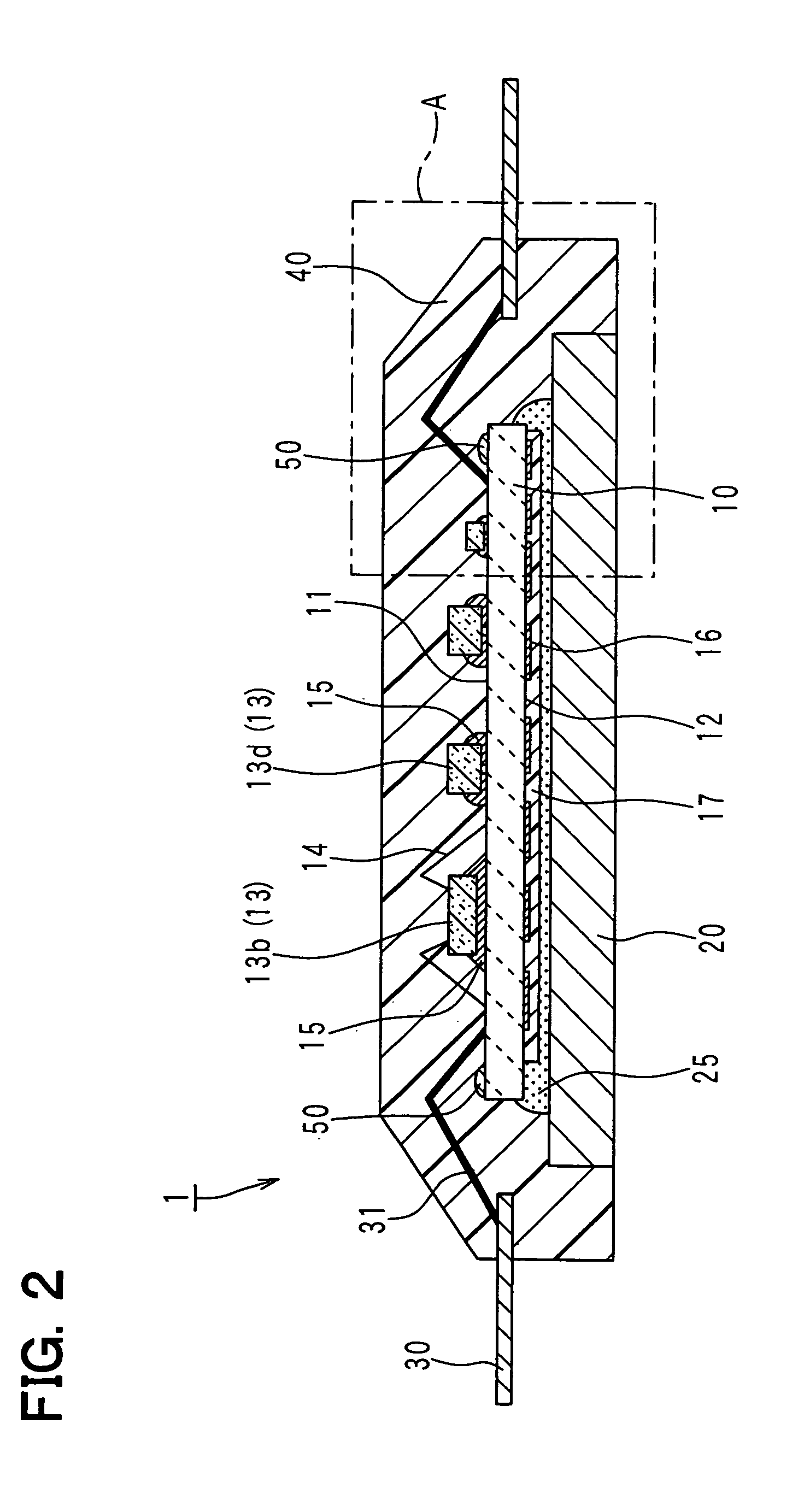
[0048]FIG. 1 is a plan view of the electronic control device according to the present embodiment. FIG. 2 is a cross-sectional view taken along line II-II in FIG. 1. A part of a molding resin 40 is not shown in FIG. 1. A configuration of an electronic control device 1 will be described with reference to FIGS. 1 and 2.

[0049]As shown in FIG. 1, the electronic control device 1 is a molding package having a square-plate shape. As shown in FIGS. 1 and 2, the electronic control device 1 is constru...

second embodiment

[0097]In the present embodiment, only a different part from the first embodiment will be described. FIG. 7 is an enlarged view of a portion of the electronic control device 1 according to the present embodiment, and corresponds to the portion A shown in FIG. 2.

[0098]As shown in FIG. 7, the electrically-conductive adhesive 50 is formed also on a lateral surface 18 of the circuit board 10. Specifically, the electrically-conductive adhesive 50 completely covers a corner portion configured by the first surface 11 and the lateral surface 18 adjacent to the first surface 11, and the electrically-conductive adhesive 50 is coated with the adhesion improving member 60.

[0099]The peeling stress in the molding resin 40 is generated from the outer edge portion 11a including the lateral surface 18 toward the center of the circuit board 10. However, because the corner portion of the circuit board 10 is completely covered by the electrically-conductive adhesive 50 and the adhesion improving member ...

third embodiment

[0100]In the present embodiment, only a different part from the first embodiment will be described. FIG. 8 is an enlarged view of a portion of the electronic control device 1 according to the present embodiment, and corresponds to the portion A shown in FIG. 2. As shown in FIG. 8, the electrically-conductive adhesives 50 are arranged in two rows, and the electrically-conductive adhesives 50 are coated with the adhesion improving member 60.

[0101]In the case where the electrically-conductive adhesives 50 are arranged in multiple rows, the adhesion improving member 60 is more likely to accumulate between the adjacent electrically-conductive adhesives 50. Thus, the adhesion improving member 60 can be thickened, and the effect of reducing the stress can be improved.

[0102]The configuration of the electrically-conductive adhesives 50 is not limited to two rows. As far as a space for the outer edge portion 11a of the first surface 11 is available, the electrically-conductive adhesives 50 ma...


PUM

PropertyMeasurementUnit
elastic modulusaaaaaaaaaa

Abstract

In an electronic control device, an electrically-conductive adhesive is arranged on an outer edge portion of a first surface of a circuit board as a stress reducing portion for reducing stress of the circuit board received by a molding resin. An elastic modulus of the electrically-conductive adhesive is lower than that of the circuit board. The electrically-conductive adhesive is covered by an adhesion improving member. When peeling stress is applied to the circuit board from the molding resin, the electrically-conductive adhesive and the adhesion improving member receive the peeling stress to be deformed. Therefore, the peeling stress to the circuit board is reduced.

Description

CROSS REFERENCE TO RELATED APPLICATION[0001]The present application is based on Japanese Patent Applications No. 2008-269457 filed on Oct. 20, 2008, and No. 2009-132257 filed on Jun. 1, 2009, the disclosures of which are incorporated herein by reference.FIELD OF THE INVENTION[0002]The present invention relates to an electronic control device molded with a sealing resin (hereinafter, referred to as a molding resin). In the electronic control device, a circuit board is fixedly bonded to a surface of a base member, and an opposite surface of the surface to which the circuit board is fixedly bonded is exposed to outside.BACKGROUND OF THE INVENTION[0003]Recently, with respect to powertrain control for a vehicle, functions for performing complex control are expected to be sophisticated in order to achieve both a comfortable drive and low-fuel consumption. Furthermore, as the number of electronic control devices is increased, the number of wiring harnesses may be increased and securing a s...

Claims


Application Information

Patent Timeline
Patent Type & Authority Patents(United States)
IPC IPC(8): H05K7/00H01L23/495
CPCH01L24/49H05K3/284H05K5/065H05K7/20454H05K1/0271H05K1/095H01L2224/4903H01L2224/45015H01L2924/19106H01L2924/15159H01L2224/45144H01L2224/45124H01L2924/19107H01L2924/19105H01L2224/73265H01L2224/48227H01L2224/32225H05K2203/1316H05K3/321H05K2201/09145H05K2201/09781H05K2201/10287H05K2203/049H01L2924/00H01L2924/00012H01L2924/00014H01L2924/2076H01L2924/15787H01L2924/181H01L24/45H01L24/73H01L24/48H01L2224/05599
Inventor KASHIWAZAKI, ATSUSHITANAKA, YASUMITSU
Owner DENSO CORP
Why Eureka
Try Eureka