Solid-state image capturing device, method of manufacturing solid-state image capturing device, and image capturing apparatus

a technology of solid-state image and capturing device, which is applied in the direction of television system scanning details, radioation control devices, television systems, etc., to achieve the effect of improving sensitivity, and inhibiting the reduction of the occupation area of the photoelectric conversion section

Active Publication Date: 2013-02-05
SONY SEMICON SOLUTIONS CORP
View PDF2 Cites 7 Cited by
  • Summary
  • Abstract
  • Description
  • Claims
  • Application Information

AI Technical Summary

Benefits of technology

[0012]It is desirable to prevent the occupation area of a photoelectric conversion unit (photodiode) from being reduced with a reduction of a pixel size and to enable improved sensitivity by forming a gate electrode of a pixel transistor section so as not to overlap on an isolation area.
[0014]In the solid-state image capturing device according to the embodiment of the invention, since the first gate electrode of the transistor is formed between the insulating sections of the isolation areas, the first gate electrode is formed so as not to overlap on the isolation areas. Accordingly, the occupation area of the photoelectric conversion section is inhibited from being reduced with the miniaturization of a pixel size, and thus the sensitivity is inhibited from deteriorating. Alternatively, the sensitivity can be improved.
[0016]In the method of manufacturing the solid-state image capturing device according to the embodiment of the invention, since the first gate electrode of the transistor is formed between the insulating sections of the isolation areas, the first gate electrode of the pixel transistor section is formed so as not to overlap on the isolation areas. Accordingly, the occupation area of the photoelectric conversion section is inhibited from being reduced with the miniaturization of a pixel size, and thus the sensitivity is inhibited from deteriorating. Alternatively, the sensitivity can be improved.
[0019]In the solid-state image capturing device according to the embodiment of the invention, the first gate electrode of the pixel transistor section is formed so as not to overlap on the isolation areas. With such a configuration, there are advantages that the occupation area of the photoelectric conversion section is inhibited from being reduced with the reduction in a pixel size and the sensitivity is improved.
[0020]In the method of manufacturing the solid-state image capturing device according to the embodiment of the invention, the first gate electrode of the pixel transistor section is formed so as not to overlap on the isolation areas. With such a configuration, there are advantages that the occupation area of the photoelectric conversion section is inhibited from being reduced with the reduction in a pixel size and the sensitivity is improved.
[0021]The image capturing apparatus according to the embodiment of the invention uses the solid-state image capturing device according to the embodiment of the invention which is capable of forming an image with high sensitivity even when a pixel size is reduced. Accordingly, an advantage of forming an image with high sensitivity is obtained.

Problems solved by technology

A problem to be solved is that when a gate electrode of a peripheral circuit section is formed to overlap on an isolation area to take the contact with the reduction in a pixel size, a gate electrode of a pixel transistor section is also formed to overlap on the isolation area.

Method used


Image

  • Solid-state image capturing device, method of manufacturing solid-state image capturing device, and image capturing apparatus
  • Solid-state image capturing device, method of manufacturing solid-state image capturing device, and image capturing apparatus
  • Solid-state image capturing device, method of manufacturing solid-state image capturing device, and image capturing apparatus

Examples


first embodiment

First Exemplary Configuration of Solid-State Image Capturing Device

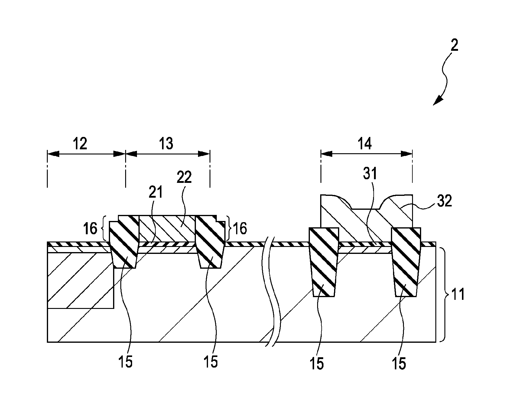
[0038]A first exemplary configuration of a solid-state image capturing device according to a first embodiment of the invention will be described with reference to a schematic sectional view of FIG. 1.

[0039]As shown in FIG. 1, a semiconductor substrate 11 is provided with a photoelectric conversion section 12 performing photoelectric conversion on incident light to obtain signal charges and a pixel transistor section 13 outputting the signal charges generated in the photoelectric conversion section 12. A peripheral circuit section 14 is formed in the periphery of a pixel section including the photoelectric conversion section 12 and the pixel transistor section 13. Isolation areas 15 are formed to electrically separate the photoelectric conversion section 12, the pixel transistor section 13, and the peripheral circuit section 14 from each other. The isolation area 15 has an insulating section 16 formed higher than the ...

second embodiment

2. Second Embodiment

First Exemplary Method of Manufacturing Solid-State Image Capturing Device

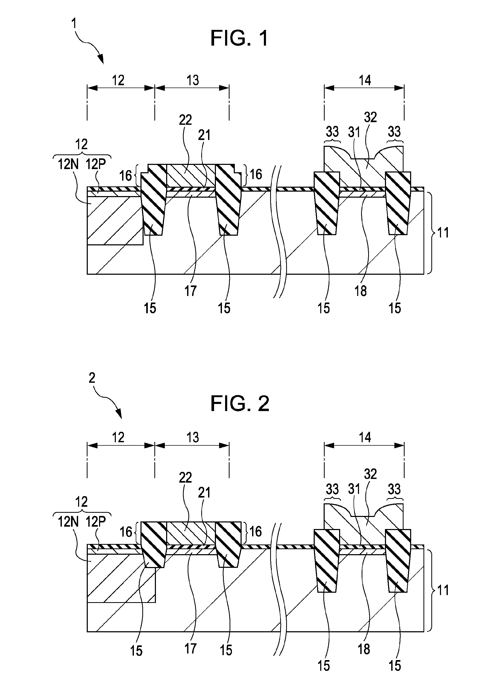
[0091]A first exemplary method of manufacturing a solid-state image capturing device according to a second embodiment of the invention will be described with reference to sectional views of FIGS. 4A to 4C and FIGS. 5A to 5C.

[0092]As shown in FIG. 4A, isolation areas 15 are formed which electrically separate a photoelectric conversion section 12, a pixel transistor section 13, and a peripheral circuit section 14 from each other formed on a semiconductor substrate 11 and which each include an insulating section 16 formed higher than the surface of the semiconductor substrate 11.

[0093]The semiconductor substrate 11 is formed of a general silicon substrate, for example. The photoelectric conversion section 12 includes an N type area 12N and a P+ type area 12P formed on the N type area 12N.

[0094]The isolation area 15 has an STI (Shallow Trench Isolation) structure, for example. In the manufactur...

third embodiment

Exemplary Configuration of Image Capturing Apparatus

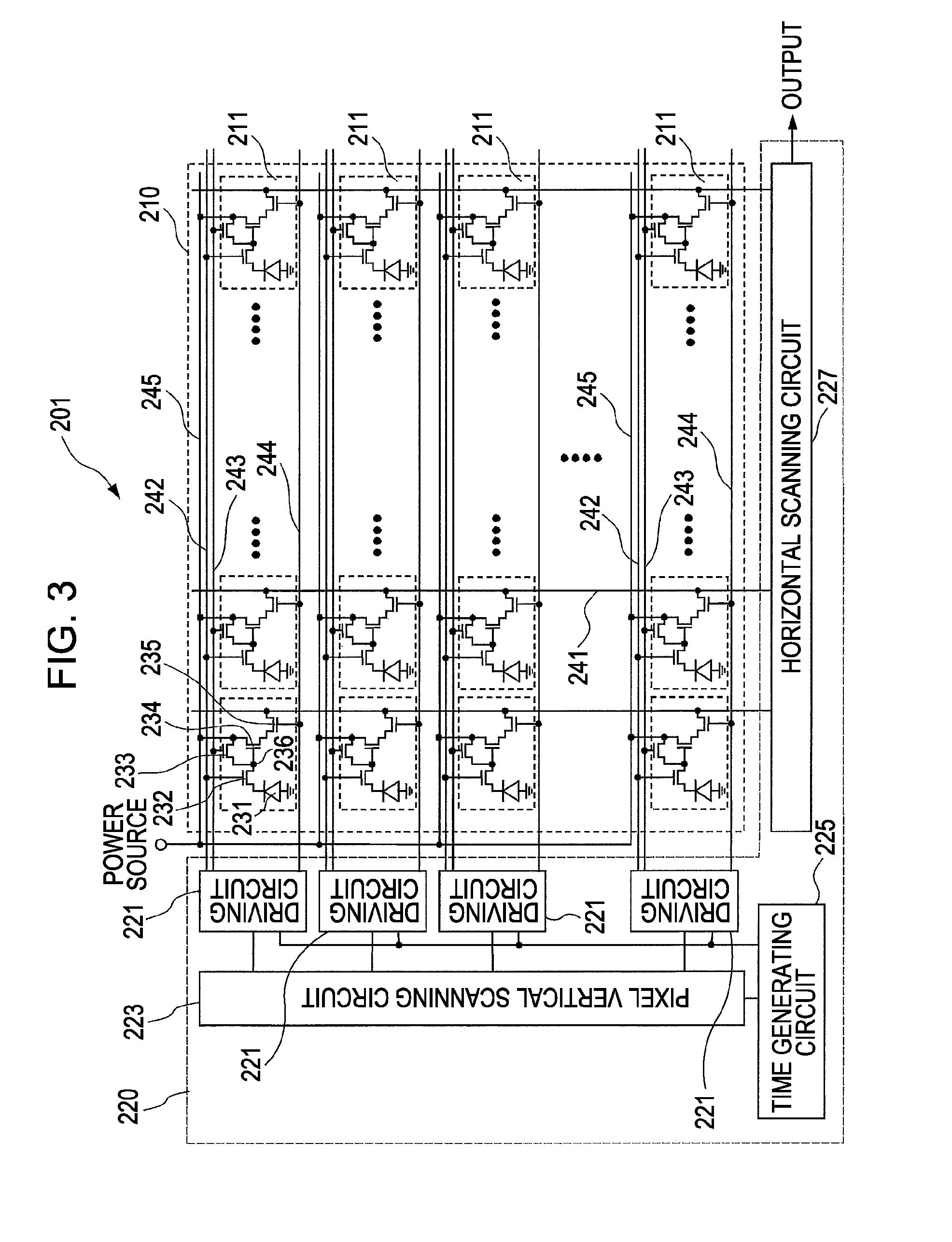
[0164]Next, an image capturing apparatus according to an embodiment of the invention will be described with reference to a block diagram of FIG. 12. The solid-state image capturing device according to the embodiments of the invention is used in the image capturing apparatus.

[0165]As shown in FIG. 12, an image capturing apparatus 300 includes the solid-state image capturing device (not shown) in an image capturing unit 301. On the light condensing side of the image capturing unit 301, there is provided a light condensing optical unit 302 forming an image. A signal processing unit 303 including a driving circuit configured to drive the image capturing unit 301 and a signal processing circuit configured to process image signals subjected to photoelectric conversion by the solid-state image capturing device. The image signals processed by the signal processing unit 303 may be stored in an image memory (not shown). For the image capturi...


PUM


Abstract

A solid-state image capturing device includes, in a semiconductor substrate, a photoelectric conversion section which performs photoelectric conversion on incident light to obtain signal charges; a pixel transistor section which outputs the signal charges generated in the photoelectric conversion section; a peripheral circuit section which is formed in the periphery of a pixel section including the photoelectric conversion section and the pixel transistor section; and isolation areas which electrically separate the photoelectric conversion section, the pixel transistor section, and the peripheral circuit section from each other. The isolation areas in the periphery of the pixel transistor section each have an insulating section formed higher than a surface of the semiconductor substrate. A first gate electrode of a transistor of the pixel transistor section is formed between the insulating sections and on the semiconductor substrate with a gate insulating film interposed therebetween.

Description

BACKGROUND OF THE INVENTION[0001]1. Field of the Invention[0002]The present invention relates to a solid-state image capturing device, a method of manufacturing the solid-state image capturing device, and an image capturing apparatus.[0003]2. Description of the Related Art[0004]With the miniaturization of each pixel of a CMOS image sensor, the area of a pixel transistor with respect to a photodiode in a unit pixel becomes larger.[0005]When a ratio of the area of the pixel transistor in the unit pixel becomes larger, the area of the photodiode becomes smaller. For this reason, a problem with a reduction in sensitivity may arise. As shown in FIG. 13, some (for example, oblique incident light) of light L incident on gate electrodes 120 of the pixel transistor may be reflected or absorbed. Therefore, due to a reduction in light arriving to the photodiode 110, the problem of the deterioration in sensitivity may arise.[0006]Since it is necessary to ensure the area corresponding to an over...

Claims


Application Information

Patent Timeline
Patent Type & Authority Patents(United States)
IPC IPC(8): H01L21/337H01L21/76H01L27/146H04N5/335H04N5/369H04N5/374
CPCH01L27/1463H01L27/14689H01L27/14603
Inventor KOGA, FUMIHIKOKUDOH, YOSHIHARU
Owner SONY SEMICON SOLUTIONS CORP
Why Eureka
Try Eureka