

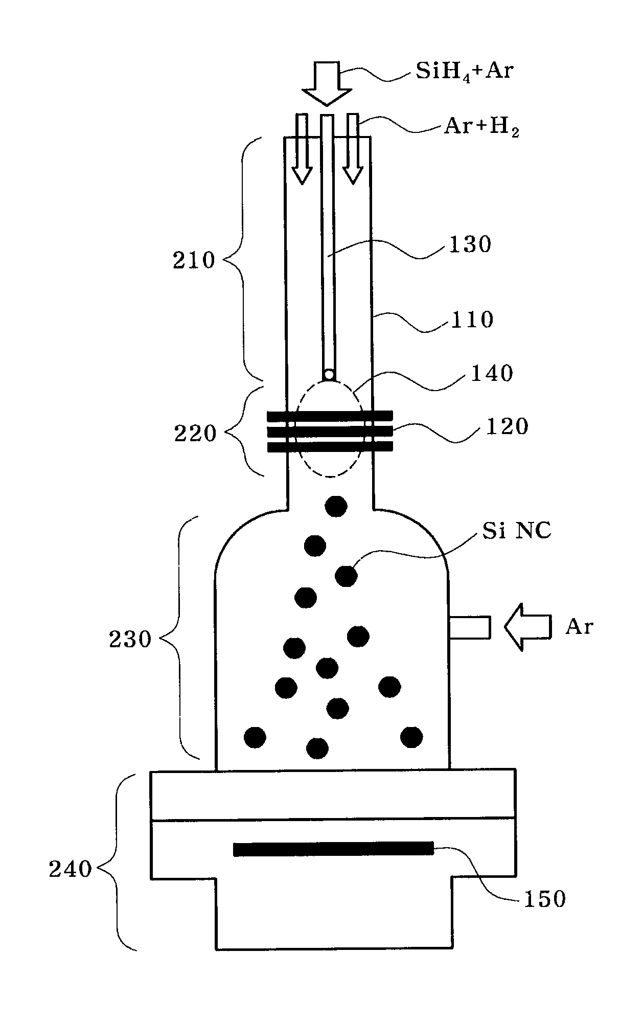
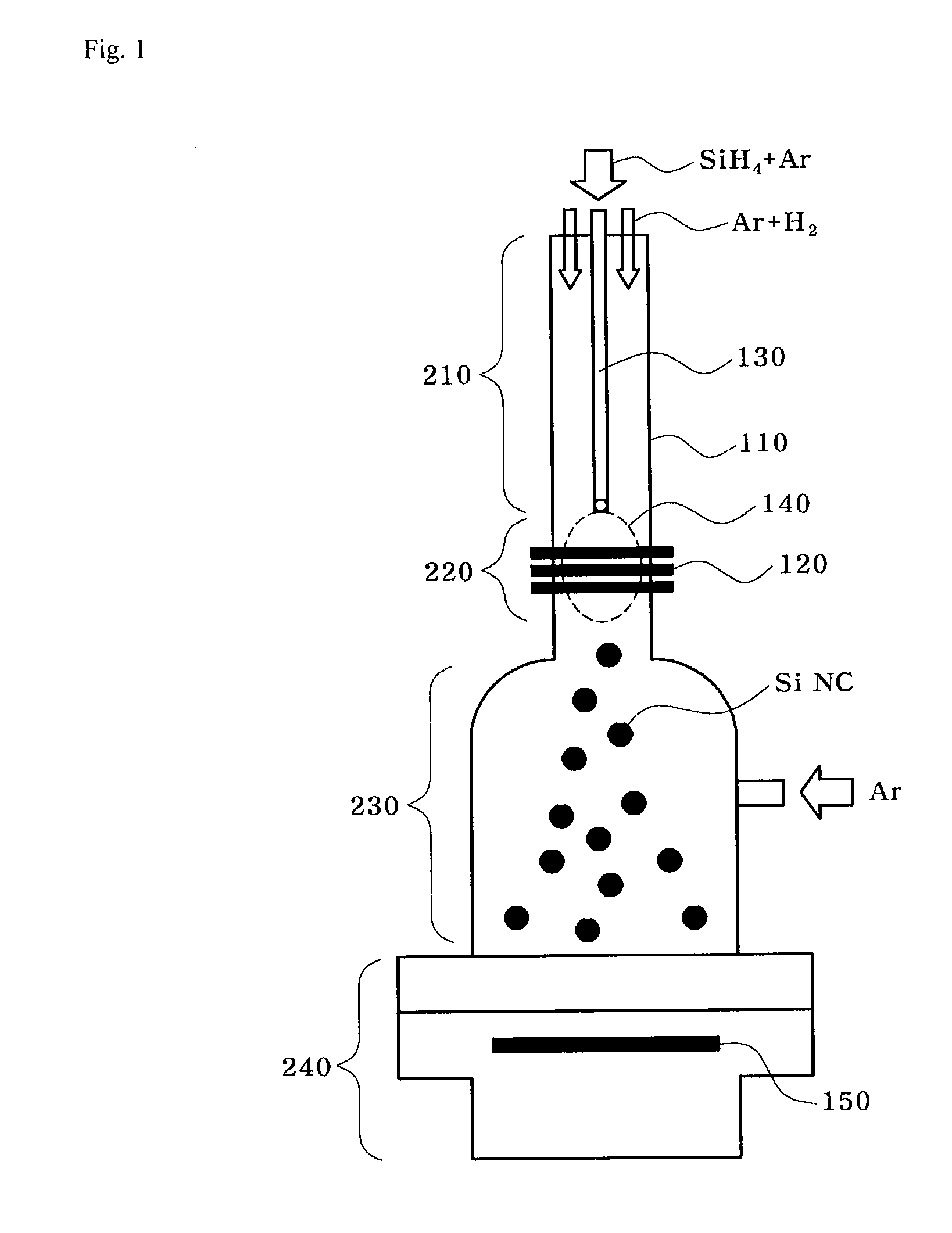
Apparatus for producing silicon nanocrystals using inductively coupled plasma
a technology of inductively coupled plasma and apparatus, which is applied in the direction of silicon compounds, silicon layered products, cellulosic plastic layered products, etc., can solve the problems of high manufacturing cost, low quality, and severe difficulty in controlling the particle size of the nanocrystal, so as to improve the particle size characteristics and quality of the silicon nanocrystals, the effect of reducing plasma diffusion
- Summary
- Abstract
- Description
- Claims
- Application Information
AI Technical Summary
Benefits of technology
Problems solved by technology
Method used
Image

Examples
examples
[0047]An alternating current of 13.56 MHz was applied with a power of 50-200 W to a coil for producing ICP. With a tube inserted into a reactor, silane and argon gases were supplied as primary gases to the reactor through the interior of the tube while changing a flow ratio of silane and argon in the range of 1:99˜10:390. As secondary gases for surface treatment of produced silicon nanocrystals, hydrogen and argon gases were supplied to the reactor along an outer surface of the tube while changing a flow ratio of hydrogen and argon in the range of 1:99˜10:90. For cooling a dispersing part, argon was separately supplied at a flow rate of 100 sccm into the reactor. The nanocrystals were produced while changing the total flow rate of the gases in the range of 300500 sccm. At this time, the tube was made of quartz and was spaced 1 cm above the uppermost end of the coil to supply the primary gases.
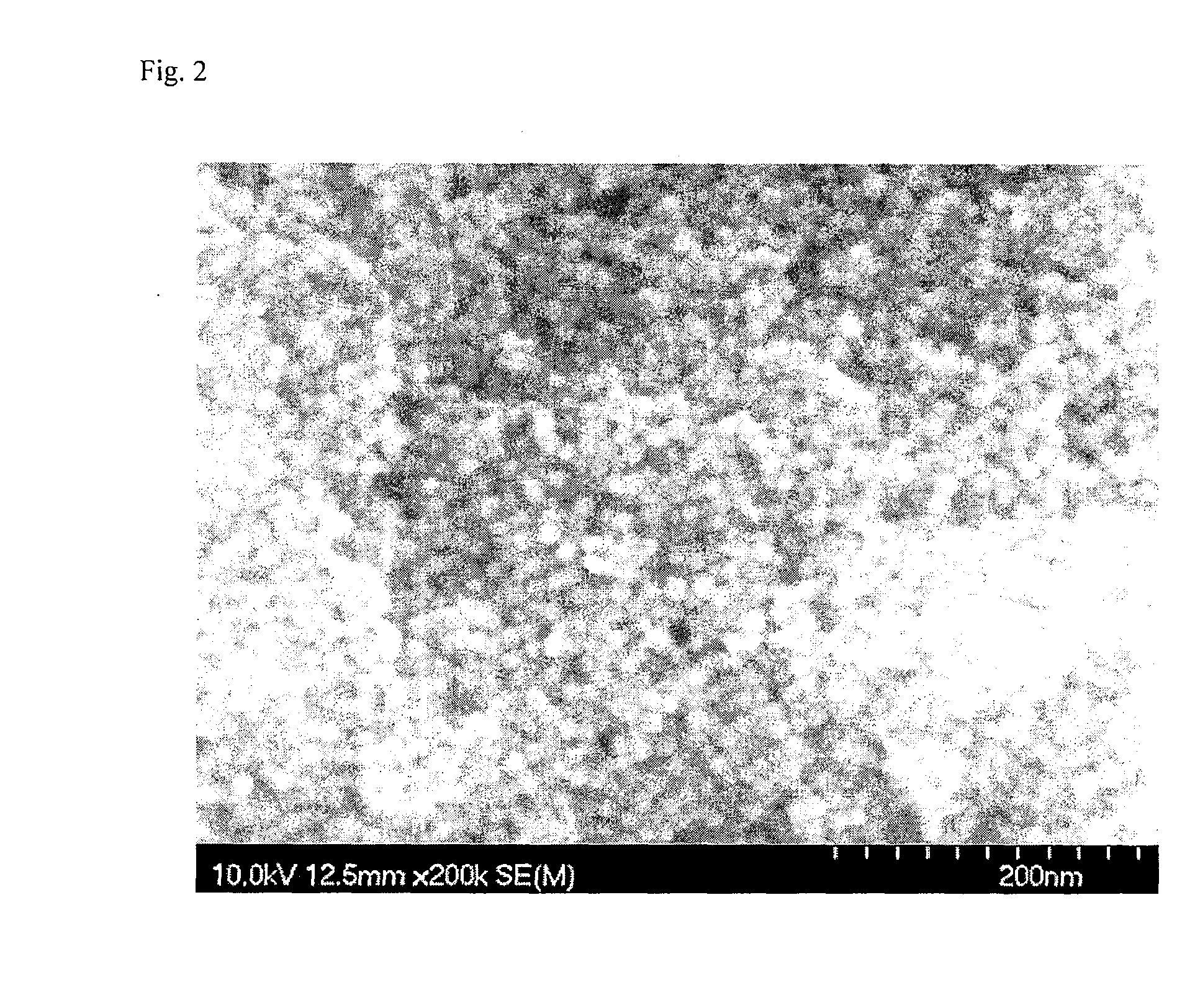
[0048]Table 1 shows particle sizes and crystallinity of silicon nanocrystals produced under...
PUM
| Property | Measurement | Unit |
|---|---|---|
| particle size | aaaaa | aaaaa |
| main wavelength | aaaaa | aaaaa |
| particle size | aaaaa | aaaaa |
Abstract
Description
Claims
Application Information