
Apparatus for producing silicon nanocrystals using inductively coupled plasma

Active Publication Date: 2010-08-12
KOREA INST OF ENERGY RES
View PDF4 Cites 5 Cited by
  • Summary
  • Abstract
  • Description
  • Claims
  • Application Information

AI Technical Summary

Benefits of technology

[0014]The present invention is conceived to solve the problems of the related art, and an aspect of the invention is to provide an apparatus for producing silicon nanocrystals, which can minimize plasma diffusion inside a reactor in production of the silicon nanocrystals using inductively coupled high-density plasma by vapor state reaction, thereby improving the particle size characteristics and quality of the silicon nanocrystals.
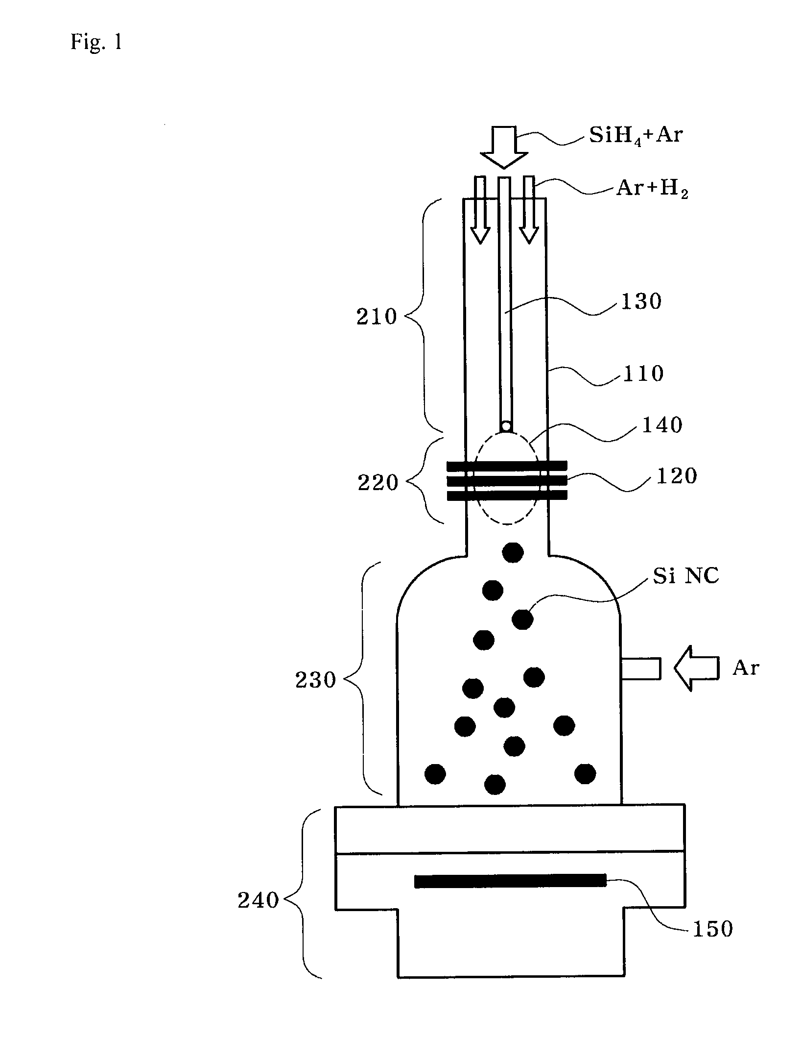
[0016]In accordance with another embodiment of the invention, an apparatus for producing silicon nanocrystals includes: a gas supply part, into which a tube is inserted to allow a primary gas for forming silicon nanocrystals and a secondary gas for surface reaction of the silicon nanocrystals to be separately supplied through an inner side and an outer side of the tube, respectively; a reactor part located below the gas supply part and having an ICP coil wound around an outer wall thereof; a dispersing part located below the reactor part to rapidly cool and disperse the silicon nanocrystals formed in the reactor part; and a collecting part located below the dispersing part to collect the silicon nanocrystals.

Problems solved by technology

As such, the solid state reaction requires the heat treatment at high temperatures to form the silicon nanocrystals and incurs very high manufacturing costs due to expensive deposition equipment.
The liquid state reaction has severe difficulty in controlling the particle size of the nanocrystals and incurs low quality in terms of crystallinity and the like.
However, the conventional ICP-based apparatus has a wide plasma reaction area caused by plasma diffusion inside the reactor.
As a result, it becomes difficult to control the particle size of the silicon nanocrystals.
The plasma diffusion also causes a wide reaction area of the secondary gas and extends reaction time, thereby deteriorating quality of the silicon nanocrystals.

Method used


Image

  • Apparatus for producing silicon nanocrystals using inductively coupled plasma
  • Apparatus for producing silicon nanocrystals using inductively coupled plasma
  • Apparatus for producing silicon nanocrystals using inductively coupled plasma

Examples


examples

[0047]An alternating current of 13.56 MHz was applied with a power of 50-200 W to a coil for producing ICP. With a tube inserted into a reactor, silane and argon gases were supplied as primary gases to the reactor through the interior of the tube while changing a flow ratio of silane and argon in the range of 1:99˜10:390. As secondary gases for surface treatment of produced silicon nanocrystals, hydrogen and argon gases were supplied to the reactor along an outer surface of the tube while changing a flow ratio of hydrogen and argon in the range of 1:99˜10:90. For cooling a dispersing part, argon was separately supplied at a flow rate of 100 sccm into the reactor. The nanocrystals were produced while changing the total flow rate of the gases in the range of 300500 sccm. At this time, the tube was made of quartz and was spaced 1 cm above the uppermost end of the coil to supply the primary gases.

[0048]Table 1 shows particle sizes and crystallinity of silicon nanocrystals produced under...


PUM

PropertyMeasurementUnit
Particle sizeaaaaaaaaaa
Timeaaaaaaaaaa
Timeaaaaaaaaaa

Abstract

The present disclosure relates to an apparatus for producing silicon nanocrystals, which can minimize plasma diffusion by finely adjusting a plasma region created by an ICP coil. The apparatus includes a reactor having an ICP coil wound around an outer wall thereof and a tube inserted into the reactor, wherein a primary gas for forming silicon nanocrystals and a secondary gas for surface reaction of the silicon nanocrystals are separately supplied to the reactor through an inner side and an outer side of the tube, respectively.

Description

BACKGROUND OF THE INVENTION[0001]1. Field of the Invention[0002]The present invention relates to an apparatus for producing silicon nanocrystals based on inductively coupled plasma (ICP) and, more particularly, to an apparatus for producing silicon nanocrystals, which can minimize plasma diffusion by finely adjusting a plasma region created by an ICP coil.[0003]2. Description of the Related Art[0004]Recently, silicon nanocrystals have been generally used as photoelectric conversion / photo conversion materials such as solar cells or light emitting devices (LEDs). Silicon is an environmentally friendly material, abundant in the Earth's crust and is utilized for various applications in the field of electronic materials. Although silicon exhibits very undesirable optical characteristics in a bulk sate, silicon nanocrystals exhibit highly efficient optical characteristics.[0005]A method of producing silicon nanocrystals can generally be classified into solid state reaction, liquid state r...

Claims


Application Information

Patent Timeline
IPC IPC(8): B01J19/08B32B5/16
CPCB01J19/088B01J2219/0883B01J2219/0894B82Y30/00Y10T428/2982C01B33/027H05H1/24Y10T117/1008Y10T117/10B82Y40/00H05H1/46H05H1/4652C08L101/10B82B3/00
Inventor JANG, BO-YUNKO, CHANG-HYUNLEE, JEONG-CHULKIM, JOON-SOOPARK, JOO-SEOK
Owner KOREA INST OF ENERGY RES
Learn More