
Optical Waveguide Amplifier Using High Quantum Efficiency Silicon Nanocrystal Embedded Silicon Oxide

a technology of nanocrystals and optical waveguides, applied in the field of optical devices, can solve problems such as poor system performance, and achieve the effect of enhancing sensing and boosting signal levels

Active Publication Date: 2009-02-12
SHARP KK
View PDF10 Cites 3 Cited by
  • Summary
  • Abstract
  • Description
  • Claims
  • Application Information

AI Technical Summary

Benefits of technology

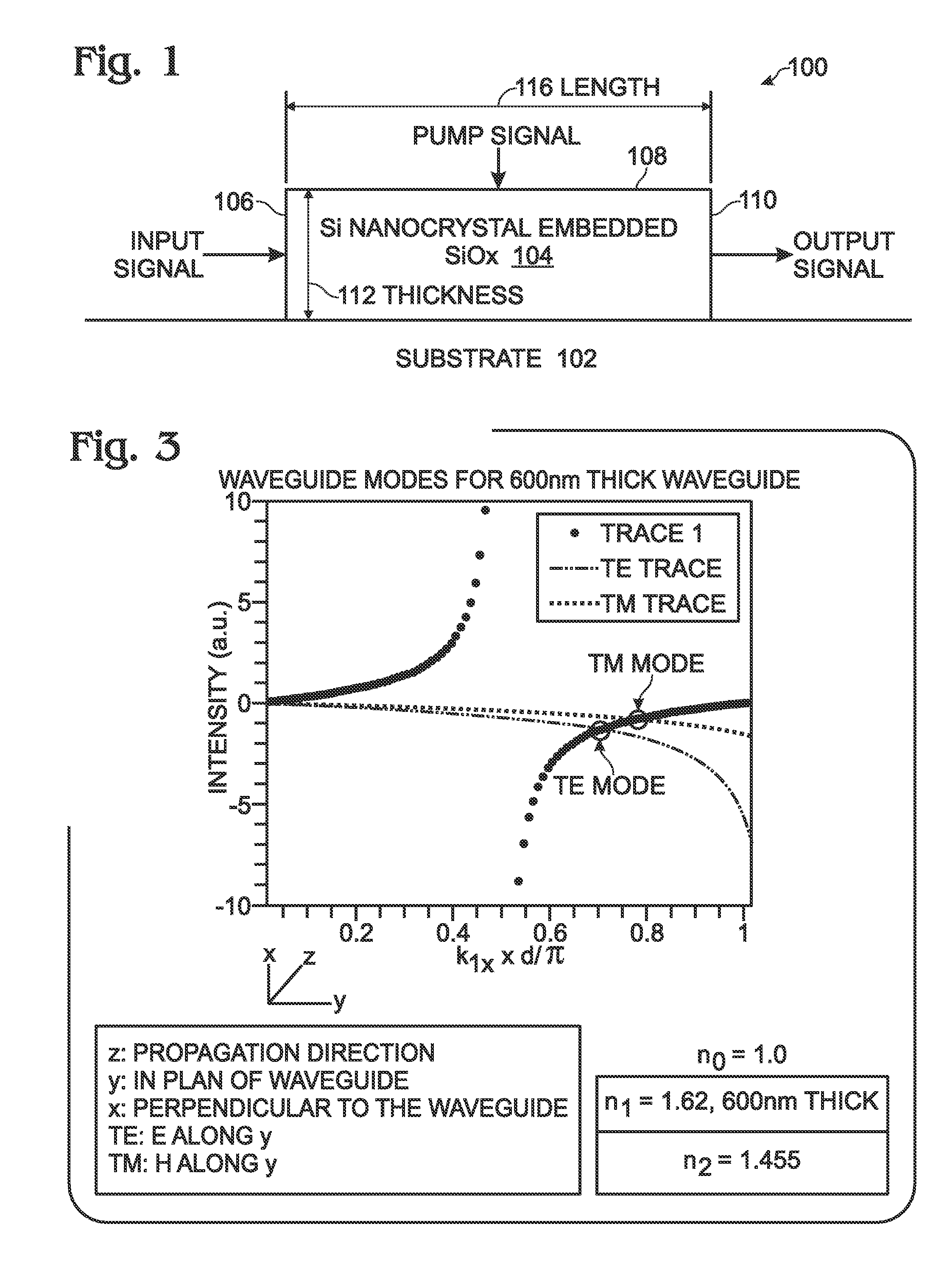
[0022]Described herein is an optical waveguide amplifier using a newly developed high quantum efficiency silicon (Si) nanocrystal embedded Si oxide (SiOx) film as a gain material for wavelengths near 750 nanometers (nm). The intensity decay of optical signals, due to absorption and scattering, can result in poor system performance. The instant waveguide enables longer-reach optical signal propagation and increases the power budget in optical system designs. In one aspect, guide modes for Si nanocrystal embedded SiOx thin films with a thickness of about 600 nm are sandwiched between a substrate and air. At this thickness, and as based upon calculation from optical waveguiding theory, one TE and one TM modes are supported in the waveguide.
[0024]This optically pumped waveguide amplifier can be used in communications between integrated optical circuits. The waveguide can also be used before photo-detectors as a preamplifier to boost signal levels above detection limits, especially for amorphous Si (α-Si) based photodetectors, to enhance sensing beyond the cut-off wavelength above 750 nm.

Problems solved by technology

The intensity decay of optical signals, due to absorption and scattering, can result in poor system performance.

Method used


Image

  • Optical Waveguide Amplifier Using High Quantum Efficiency Silicon Nanocrystal Embedded Silicon Oxide
  • Optical Waveguide Amplifier Using High Quantum Efficiency Silicon Nanocrystal Embedded Silicon Oxide
  • Optical Waveguide Amplifier Using High Quantum Efficiency Silicon Nanocrystal Embedded Silicon Oxide

Examples


Embodiment Construction

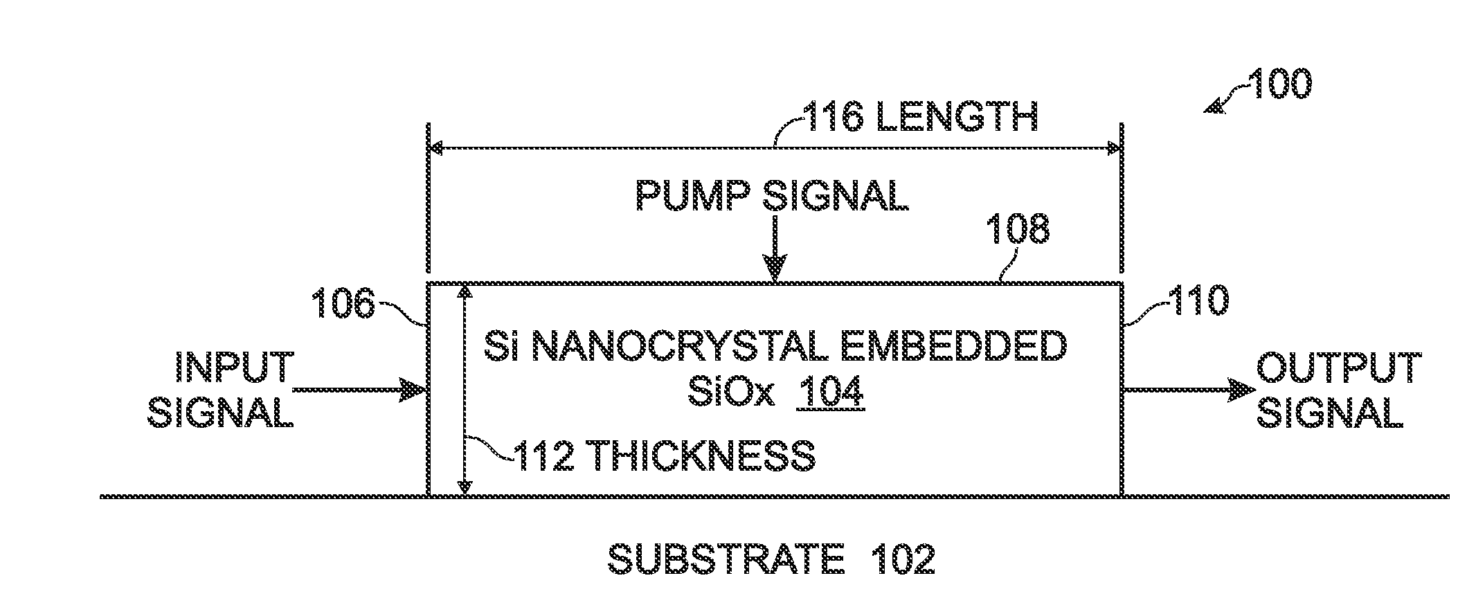
[0039]FIG. 1 is a partial cross-sectional view of a silicon (Si) nanocrystal embedded silicon oxide (SiOx) waveguide. The waveguide 100 comprises a bottom substrate 102 having an optical index. For example, the substrate 102 may be silicon dioxide. A Si nanocrystal embedded SiOx strip 104, where x is less than 2, overlies the bottom substrate. The Si nanocrystal embedded SiOx strip 104 has an optical index greater than the underlying (bottom substrate) optical index, and a first interface 106 accept an optical input signal with a first power at a first wavelength in a range of 700 to 950 nanometers (nm). Typically, the Si nanocrystal embedded SiOx waveguide 104 has an optical index in the range of about 1.58 to 1.75.

[0040]The Si nanocrystal embedded SiOx strip 104 has a second interface 108 to accept an optical source pump signal having a second power at a second wavelength in the range of 250 to 550 nm, and a third interface 110 to supply an optical output signal having a third, po...


PUM

PropertyMeasurementUnit
Temperatureaaaaaaaaaa
Lengthaaaaaaaaaa
Lengthaaaaaaaaaa

Abstract

A method is provided for optical amplification using a silicon (Si) nanocrystal embedded silicon oxide (SiOx) waveguide. The method provides a Si nanocrystal embedded SiOx waveguide, where x is less than 2, having a quantum efficiency of greater than 10%. An optical input signal is supplied to the Si nanocrystal embedded SiOx waveguide, having a first power at a first wavelength in the range of 700 to 950 nm. The Si nanocrystal embedded SiOx waveguide is pumped with an optical source having a second power at a second wavelength in a range of 250 to 550 nm. As a result, an optical output signal having a third power is generated, greater than the first power, at the first wavelength. In one aspect, the third power increases in response to the length of the waveguide strip.

Description

RELATED APPLICATIONS[0001]This application is a continuation-in-part of a pending patent application entitled, SILICON NANOCRYSTAL EMBEDDED SILICON OXIDE ELECTROLUMINESCENCE DEVICE WITH A MID-BANDGAP TRANSITION LAYER, invented by Huang et al. Ser. No. 12 / 197,045 filed on Aug. 22, 2008, Attorney Docket No. SLA2297, which is a Continuation-in-Part of:[0002]pending patent application, LIGHT EMITTING DEVICE WITH A NANOCRYSTALLINE SILICON EMBEDDED INSULATOR FILM, invented by Huang et al. Ser. No. 12 / 126,430, filed on May 23, 2008, Attorney Docket No, SLA2270, which is a Continuation-in-Part of the following applications:[0003]SILICON OXIDE THIN-FILMS WITH EMBEDDED NANOCRYSTALLINE SILICON, invented by Pooran Joshi et al, Ser. No. 11 / 418,273, Attorney Docket No. SLA0963, filed May 4, 2006;[0004]ENHANCED THIN-FILM OXIDATION PROCESS, invented by Pooran Joshi et al., Ser. No. 11 / 327,612, Attorney Docket-No. SLA8012, filed Jan. 6, 2006;[0005]HIGH-DENSITY PLASMA HYDROGENATION, invented by Poora...

Claims


Application Information

Patent Timeline
IPC IPC(8): H04B10/12
CPCC23C16/30C23C16/401C23C16/505C23C16/56H01S3/169H01L21/02164H01L21/02274H01L21/31608H01S3/0632G02B6/0229
Inventor HUANG, JIANDONGJOSHI, POORAN CHANDRAZHANG, HAOVOUTSAS, APOSTOLOS T.
Owner SHARP KK
Learn More