Semiconductor device

a technology of semiconductor devices and silicon vias, applied in semiconductor devices, digital storage, instruments, etc., can solve the problems of device as a whole becoming defective, not efficient, and the necessary number of through silicon vias becoming considerably large, and achieve the effect of faster transmission speed of layer address signals

Inactive Publication Date: 2013-03-19
LONGITUDE SEMICON S A R L
View PDF6 Cites 61 Cited by
  • Summary
  • Abstract
  • Description
  • Claims
  • Application Information

AI Technical Summary

Benefits of technology

[0008]The first means is to use plural through silicon vias in parallel for one signal. According to this means, even when one through silicon via is non-conductive, other through silicon vias can maintain a conductive state. Further, because a control that uses a switching circuit or the like is not necessary to connect the plural through silicon vias in parallel, there is an effect that a delay due to passage of a signal via the switching circuit does not occur. On the other hand, because the number of necessary through silicon vias increases, there is a disadvantage that a chip area increases.
[0009]The second means is to provide redundant through silicon vias in advance for n signal lines (n through silicon vias) instead of preparing plural through silicon vias per one signal, selectively use the n through silicon vias when there is no defect, and selectively use redundant through silicon vias when a certain through silicon via has a defect. According to this method, a defect of a product as a whole can be avoided by a relatively small area increase as compared to a case of connecting plural through silicon vias in parallel. Meanwhile, a switching circuit for selecting a through silicon via to be used is necessary, and therefore this method has a disadvantage in that a delay occurs due to passage of a signal via the switching circuit.
[0012]According to the present invention, a layer address signal is transmitted by using plural through silicon vias, and a command signal is transmitted by using a through silicon via that is selected from the plural through silicon vias. Therefore, the transmission speed of the layer address signal becomes faster than the transmission speed of the command signal. Accordingly, the layer address signal can reach each controlled chip earlier than the command signal. Even when a defect occurs in a through silicon via, this defect does not cause a defect in the whole of a semiconductor device.

Problems solved by technology

However, when signals are transmitted by using plural through silicon vias for all signals, a necessary number of through silicon vias becomes considerably large, and it is not efficient.
On the other hand, when each signal is transmitted by using one through silicon via that is allocated to each signal in a fixed manner, a device as a whole becomes defective even when one defect occurs in a through silicon via.
On the other hand, because the number of necessary through silicon vias increases, there is a disadvantage that a chip area increases.
Meanwhile, a switching circuit for selecting a through silicon via to be used is necessary, and therefore this method has a disadvantage in that a delay occurs due to passage of a signal via the switching circuit.

Method used


Image

  • Semiconductor device
  • Semiconductor device
  • Semiconductor device

Examples


Embodiment Construction

[0027]Preferred embodiments of the present invention will be explained below in detail with reference to the accompanying drawings.

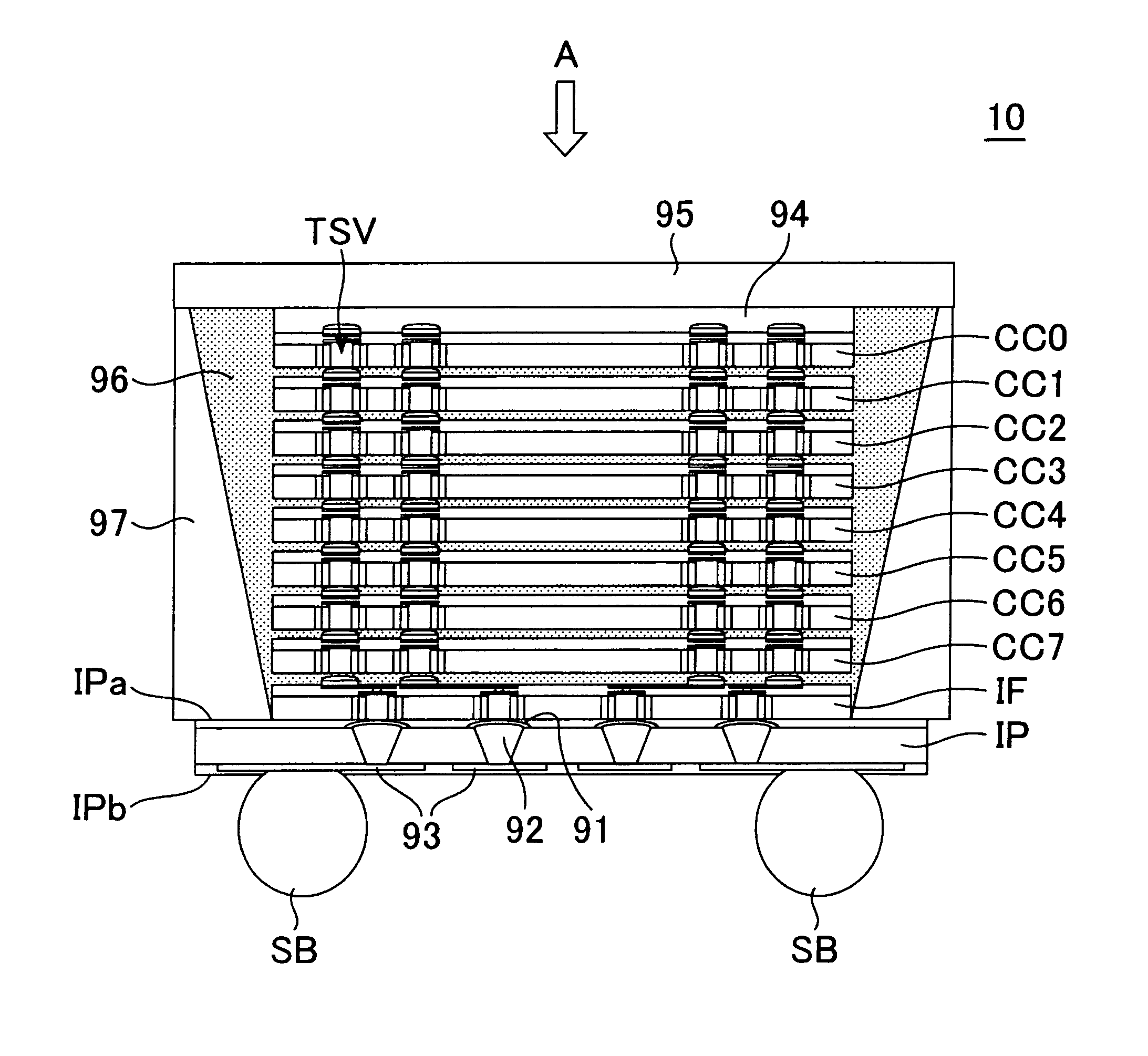
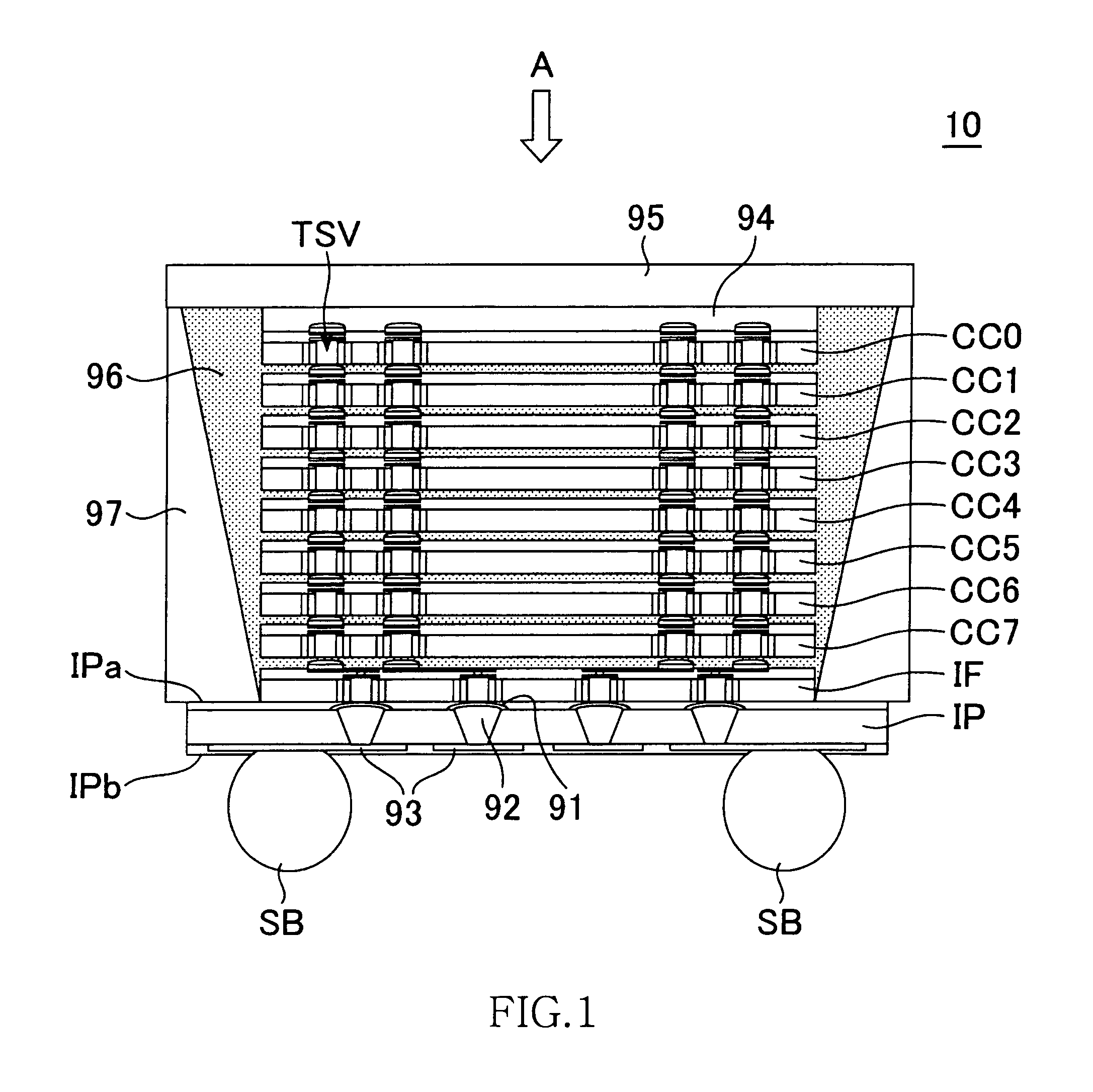
[0028]FIG. 1 is a schematic cross-sectional view provided to explain the structure of a semiconductor memory device 10 according to the preferred embodiment of the present invention.

[0029]As shown in FIG. 1, the semiconductor memory device 10 according to this embodiment has the structure where 8 core chips CC0 to CC7 that have the same function and structure and are manufactured using the same manufacture mask, an interface chip IF that is manufactured using a manufacture mask different from that of the core chips and an interposer IP are laminated. The core chips CC0 to CC7 and the interface chip IF are semiconductor chips using a silicon substrate and are electrically connected to adjacent chips in a vertical direction through plural Through Silicon Vias (TSV) penetrating the silicon substrate. Meanwhile, the interposer IP is a circuit board that is m...


PUM


Abstract

A semiconductor device according to the present invention includes plural controlled chips CC0 to CC7 that hold mutually different layer information, and a control chip IF that supplies in common layer address signals A13 to A15 and a command signal ICMD to the controlled chips. Each bit that constitutes the layer address signals A13 to A15 is transmitted via at least two through silicon vias that are connected in parallel for each controlled chip out of plural first through silicon vias. Each bit that constitutes the command signal ICMD is transmitted via one corresponding through silicon via that is selected by an output switching circuit and an input switching circuit. With this configuration, the layer address signals A13 to A15 reach the controlled chips earlier than the command signal ICMD.

Description

BACKGROUND OF THE INVENTION[0001]1. Field of the Invention[0002]The present invention relates to a semiconductor device, and more particularly relates to a semiconductor device in which a control chip and controlled chips are connected to each other via through silicon vias.[0003]2. Description of Related Art[0004]A memory capacity required for semiconductor devices such as DRAM (Dynamic Random Access Memory) has been increasing every year. In recent years, to satisfy this requirement for an increased memory capacity, there has been proposed a method of stacking plural memory chips and electrically connecting these memory chips via through silicon vias on a silicon substrate (see Japanese Patent Application Laid-open No. 2005-210106).[0005]Japanese Patent Application Laid-open No. 2005-210106 describes a semiconductor device having plural power-source through silicon vias for power source arranged to surround a periphery of a through silicon via for signal transmission. With this ar...

Claims


Application Information

Patent Timeline
Patent Type & Authority Patents(United States)
IPC IPC(8): G11C5/00G11C8/00G11C7/00
CPCG11C5/04G11C7/1072G11C8/12G11C11/4093G11C29/702G11C11/4082H01L2224/16145
Inventor YOKO, HIDEYUKI
Owner LONGITUDE SEMICON S A R L
Why Eureka
Try Eureka