Optical coupler having first and second terminal boards and first and second conversion elements

a technology of optical couplers and terminal boards, applied in the field of optical couplers, can solve the problems of preventing the merit of juxtaposed type optical couplers from being used to good effect, high manufacturing cost of optical couplers, etc., and achieve the effect of reducing the size of the semiconductor relay

Active Publication Date: 2013-04-02
ORMON CORP
View PDF14 Cites 6 Cited by
  • Summary
  • Abstract
  • Description
  • Claims
  • Application Information

AI Technical Summary

Benefits of technology

[0020]According to one or more embodiments of the present invention, a juxtaposed type optical coupler, manufacturing cost of which is low as compared with that of an opposed type optical coupler, has high values of photoelectromotive force and a photocurrent, to give favorable output efficiency.
[0022]In the optical coupler according to one or more embodiments of the present invention, even when a distance between the first conversion element and the second conversion element varies or a shape of the light reflective curved surface varies to cause displacement of a position irradiated with the optical signal that is incident on the second conversion element, the optical signal can be made incident almost uniformly on each of the light receiving cells, and also, an amount of light received in each of the light receiving cells can be held almost unchanged. Therefore, not only electromotive force and an output current (photocurrent) generated in the second conversion element can be made larger, but also the electromotive force and the output current become stable so that output characteristics of the optical coupler can be stabilized.
[0023]In the optical coupler according to the one aspect of the present embodiment, among the light receiving cells arrayed in parallel with one another, the light receiving cell located at the midsection has a narrower width and the light receiving cell located at the end has a wider width. When the first conversion element is located on the central line passing through the center of a width direction of the second conversion element or in the vicinity of the central line, optical intensity may be higher in the light receiving cell at the midsection and optical intensity is lower in the light receiving cell at the end, but in such a case, a width of the light receiving cell located at the midsection is narrowed and a width of the light receiving cell located at the end is widened so that the amount of light received in each light receiving cell can be made uniform, thereby to further enhance the output characteristics of the optical coupler.
[0024]In accordance with another aspect of the present invention, there is provided a photoelectric conversion element, including: a plurality of light receiving cells that are long in one direction; and two pads, wherein the light receiving cells are electrically connected in series and arrayed in parallel with one another, and the two pads are along with a side orthogonal to the length direction of the light receiving cells that are electrically connected respectively to both ends of the light receiving cells connected in series, and arrayed in parallel with one another. This photoelectric conversion element (light receiving cell array) can be used as the second conversion element in the optical coupler according to one or more embodiments of the present invention, and the pads can be arranged so as to be located at the farther end from the first conversion element, whereby wiring of bonding wires is not complicated in connecting the wires to the pads, an optical signal from the first conversion element is not apt to be blocked by the wires, and the light reflective curved surface is not apt to warp due to the influence of the wires in forming the light reflective curved surface on the surface of the transparent resin or the like.
[0027]The MOS driver and the semiconductor relay can be produced through use of the structure of the optical coupler according to one or more embodiments of the present invention, thus exerting similar action effects to that of the optical coupler according to one or more embodiments of the present invention. Further, since the control circuit and the MOSFETs can be integrally formed, the MOS driver and the semiconductor relay can be reduced in size.

Problems solved by technology

H5-308151 has a disadvantage that, since the surface shape of the of the transparent resin needs to be controlled with accuracy, manufacturing cost of the optical coupler is high, thereby preventing the merit of the juxtaposed type optical coupler from being used to good effect.

Method used


Image

  • Optical coupler having first and second terminal boards and first and second conversion elements
  • Optical coupler having first and second terminal boards and first and second conversion elements
  • Optical coupler having first and second terminal boards and first and second conversion elements

Examples


first embodiment

[0047](First Embodiment)

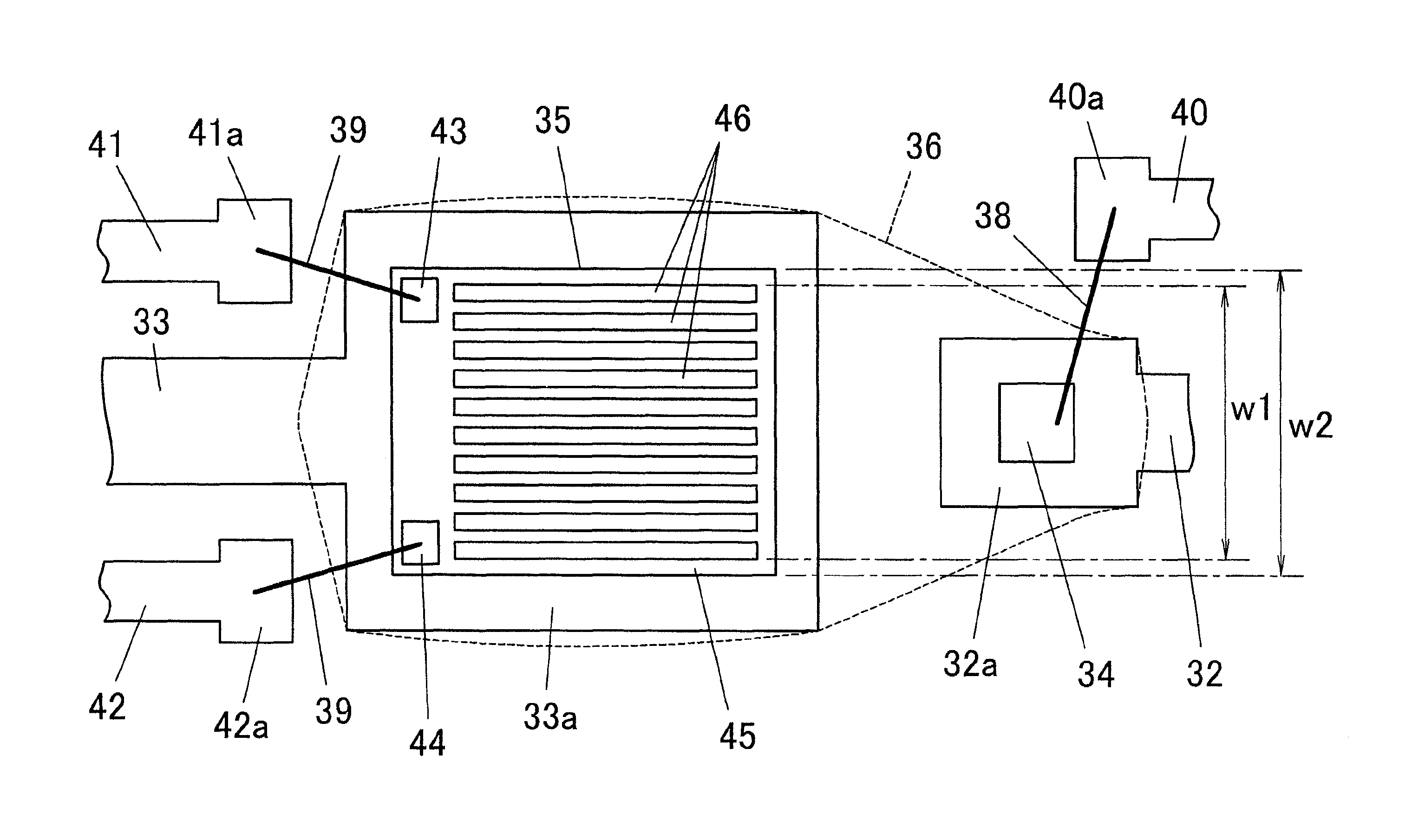
[0048]First, a structure of an optical coupler 31 of a first embodiment of the present invention will be described. FIG. 4 is a sectional view showing a structure of the optical coupler 31 in accordance with the first embodiment. FIG. 5 is a plan view showing a light emitting element 34 (first conversion element) and a light receiving element 35 (second conversion element) which are mounted on element mounting sections 32a, 33a of lead frames 32, 33 inside the optical coupler 31.

[0049]As shown in FIG. 5, the optical coupler 31 includes: the lead frame 32 (terminal board) for die-bonding of the light emitting element 34 to the element mounting section 32a; the lead frame 33 (terminal board) for die-bonding of the light receiving element 35; a lead frame 40 for wire-bonding between a wiring section 40a and the light emitting element 34; and lead frames 41, 42 for wire-bonding between wiring sections 41a, 42a and the light receiving element 35. Any of the respec...

second embodiment

[0088](Second Embodiment)

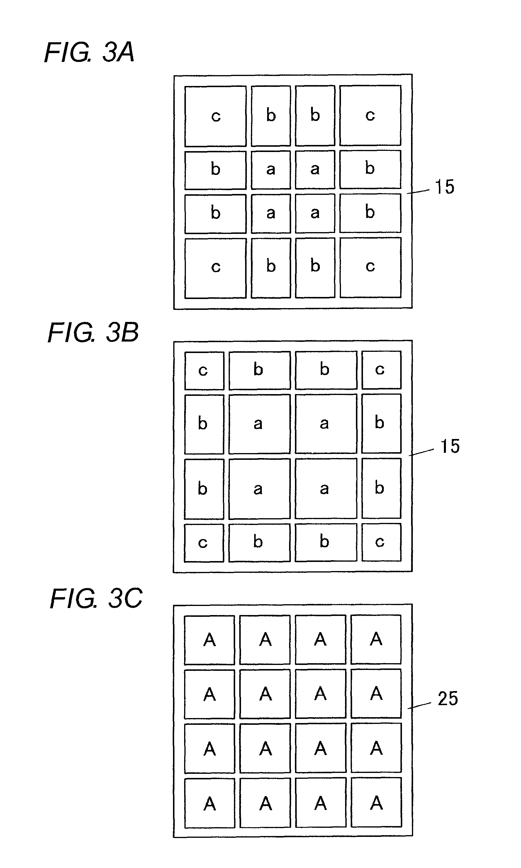
[0089]FIG. 14 is a plan view showing a structure of a principal part of an optical coupler 51 in accordance with a second embodiment of the present invention. Each of the light receiving cells 46 arrayed in parallel has an equivalent width in the optical coupler 31 of the first embodiment, whereas in the optical coupler 51, the width of the light receiving cell 46 at the midsection is narrowed and the width of the light receiving cell 46 at the end is widened. Other configurations are similar to those of the first embodiment, and descriptions thereof are thus omitted.

[0090]In the case of the light emitting element 34 being located almost on the central line of the light receiving area (whole of light receiving cells), an optical signal incident on the light receiving cell 46 at the center has larger light intensity than that of an optical signal incident on the light receiving cell 46 at each end. Therefore, in such a case, the width of the light receiving c...

third embodiment

[0092](Third Embodiment)

[0093]FIG. 15 is a sectional view showing an optical couple 52 in accordance with a third embodiment of the present invention. Also this optical coupler 52 is a juxtaposed type optical coupler since the light emitting element 34 and the light receiving element 35 are mounted on the surfaces of the same orientation in the element mounting sections 32a, 34a. Further, in this optical coupler 52, the element mounting section 32a mounted with the light emitting element 34 is higher than the element mounting section 33a mounted with the light receiving element 35.

[0094]As this optical coupler 52, when the position of the light emitting element 34 is higher than the position of the light receiving element 35, as indicated with an arrow line in FIG. 16, not only that light launched from the light emitting element 34 is reflected on the light reflective resin layer 48 and incident on the light receiving element 35, but also that part of the light launched from the lig...


PUM

PropertyMeasurementUnit
electromotive forceaaaaaaaaaa
temperatureaaaaaaaaaa

Abstract

An optical coupler has a first terminal board and a second terminal board, a first conversion element for converting an electrical signal into an optical signal mounted on a surface of a first element mounting section of the first terminal board, a second conversion element for converting an optical signal into an electrical signal mounted on a surface of a second element mounting section of the second terminal board; and a light reflective curved surface formed so as to cover the first conversion element and the second conversion element. The surfaces of the first element mounting section and the second element mounting section have the same orientation. An optical signal emitted from the first conversion element is reflected on the light reflective curved surface, to optically couple the first conversion element and the second conversion element. The second conversion element has a plurality of light receiving cells that are electrically connected in series, arrayed in parallel with one another, and longer in a longitudinal direction than in a width direction. The first conversion element is arranged inside an area sandwiched between two contact lines that are set so as to be in contact with an outline of the second conversion element, and are in parallel with a length direction of the light receiving cells.

Description

TECHNICAL FIELD[0001]The present invention relates to an optical coupler that electrically couples one terminal with the other terminal through an optical signal. Specifically, the present invention relates to an optical coupler for converting an input electrical signal into an optical signal and further converting the optical signal into an output electrical signal, thereby to electrically couple an input and an output while holding insulation therebetween.RELATED ART[0002](Two Types of Optical Couplers)[0003]FIGS. 1 and 2 show two types of optical couplers. FIG. 1 is a sectional view of an opposed type optical coupler, and FIG. 2 shows a sectional view of a juxtaposed type optical coupler.[0004]An opposed type optical coupler 11 shown in FIG. 1 is structured such that a light emitting element 14 and a light receiving element 15 mounted on lead frames 12, 13 are vertically opposed to each other, a space between the light emitting element 14 and the light receiving element 15 is sea...

Claims


Application Information

Patent Timeline
Patent Type & Authority Patents(United States)
IPC IPC(8): G02B27/00H01L31/12
CPCH01L27/1446H01L31/0203H01L31/167H01L31/173H04B10/802H01L2224/45124H01L2224/45144H01L2224/45147H01L2924/13091H01L2224/48247H01L2224/48091H01L2924/00014H01L2924/01322H01L2924/00H01L24/45H01L2924/01015H01L2924/01047H01L2924/12041H01L2924/12043H01L2924/181H01L2224/05553H01L2224/05554H01L2224/8592H01L2924/00012
Inventor OMURA, EIICHI
Owner ORMON CORP
Why Eureka
Try Eureka