Low resistance ultraviolet light emitting device and method of fabricating the same

a light-emitting device and ultraviolet light-emitting technology, which is applied in the manufacturing of semiconductor/solid-state devices, semiconductor devices, electrical devices, etc., can solve the problems of surface roughening or re-structuring type, achieve better surface roughness and film quality, and increase the lateral growth mode and crystallinity. , the effect of improving the surface roughness

Active Publication Date: 2013-04-09
NIITEK
View PDF12 Cites 3 Cited by
  • Summary
  • Abstract
  • Description
  • Claims
  • Application Information

AI Technical Summary

Benefits of technology

[0022]Still another advantage is provided in a light-emitted device. In one embodiment, the light-emitting device has a first buffer layer that is AlN with a trace amount of elemental indium and second buffer layer that is an nested superlattice structure. The nested superlattice layer may comprise a continuous gradient with an increasing Ga / Al ratio initiating at zero and terminating at the Ga / Al ratio of the n-contact layer which is selected based on the desired emission of the LED. The indium may or may not be introduced to the first buffer layer. However, elemental indium is preferably introduced to the second buffer layer. Trace amount of elemental indium provides more surface mobility for ad atoms thereby increasing the lateral growth mode and crystallinity to provide for a better surface roughness and film quality. As used herein, “trace amount of elemental indium” refers to an amount of indium that is about 1014 to about 1024 atoms of elemental indium per cm3.
[0023]Yet another advantage is provided in a light-emitting device. The light-emitting device has an ultraviolet light-emitting structure deposited on top of the buffer layers that includes a layered arrangement of an undoped or n-type AlxInyGa1-x-yN (wherein 0<x≦1 and 0≦y≦1, and 0<x+y≦1) low defect density layer(s) that is treated with silicon and indium containing precursor sources and that includes a trace amount of elemental indium, a quantum well active region with a trace amount of elemental indium, and p-type AlxInyGa1-x-yN (wherein 0≦x≦1, 0≦y≦1 and 0≦x+y≦1) and GaN materials with a trace amount of elemental indium. In one embodiment, this layer is also doped with silicon. The introduction of a trace amount of elemental indium provides for better surface mobility and migration of various ad atoms. As used herein, “ad atoms” refers to atoms that lay on a crystal surface, and that are the opposite of surface vacancy. The use of indium can increase the lateral growth mode by providing a better surface roughness and film quality such as crystallinity. Moreover, silicon and indium containing precursor source treatment for high Al based AlInGaN provides roughness to the surface through pulse cycle etching. Incorporation of indium also assists in the pacification of defects and increases silicon doping efficiency.
[0024]Yet another advantage is provided in a light-emitting device. The light-emitting device has a quantum well (MQW) active region of doped or undoped AlxInyGa1-x-yN / AlxInyGa1-x-yN with a trace amount of elemental indium. The presence of a trace amount of elemental indium increases the crystallinity of the material and improves the structural quality of the AlxInyGa1-x-yN epilayers. The trace amount of indium in the MQW layer is preferably in the range of about 0.001-5%.
[0025]Still another advantage is provided in a light-emitting device. The light-emitting device has an hole tunneling layer with magnesium as a dopant and with a trace amount of elemental indium. When magnesium is used as a dopant in typical p-type AlGaN layers for LEDs, doping is poor because of the compensation of carriers by a large number of native defects. Also, the binding energy of magnesium is higher than that for GaN. Thus, in the present invention indium is included in an amount that is just enough to compensate for the defects. The indium acts as a defect passivant. This trace amount of elemental indium will also help in lowering the binding energy of magnesium which then helps in improving doping conversion and efficiency. It is also possible that indium binds with hydrogen and thereby releases magnesium atoms for effective doping.

Problems solved by technology

This layer is subjected to silicon and indium containing precursor source treatment, which causes the formation of holes within the layer or may cause any type of surface roughening or re-structuring.

Method used


Image

  • Low resistance ultraviolet light emitting device and method of fabricating the same
  • Low resistance ultraviolet light emitting device and method of fabricating the same
  • Low resistance ultraviolet light emitting device and method of fabricating the same

Examples


Embodiment Construction

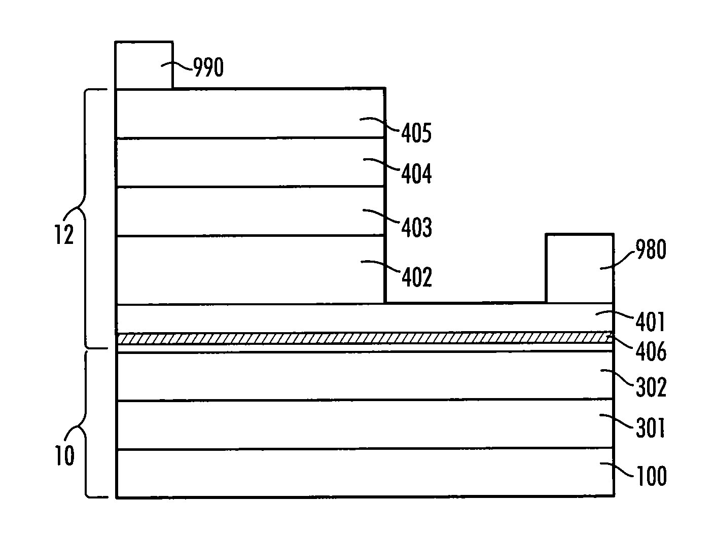
[0035]The present invention is directed to a light-emitting device (LED) and a method for making an LED, particularly one that emits deep ultraviolet light. In particular, it is directed to a template that serves as a platform for an improved ultraviolet light-emitting structure, which includes epilayers constructed to overcome high series resistance.

[0036]The invention will be described with reference to the various figures forming an integral part of the instant disclosure. The figures and descriptions thereof, refer specifically to preferred embodiments without limit thereto. Throughout the figures similar elements will be numbered accordingly.

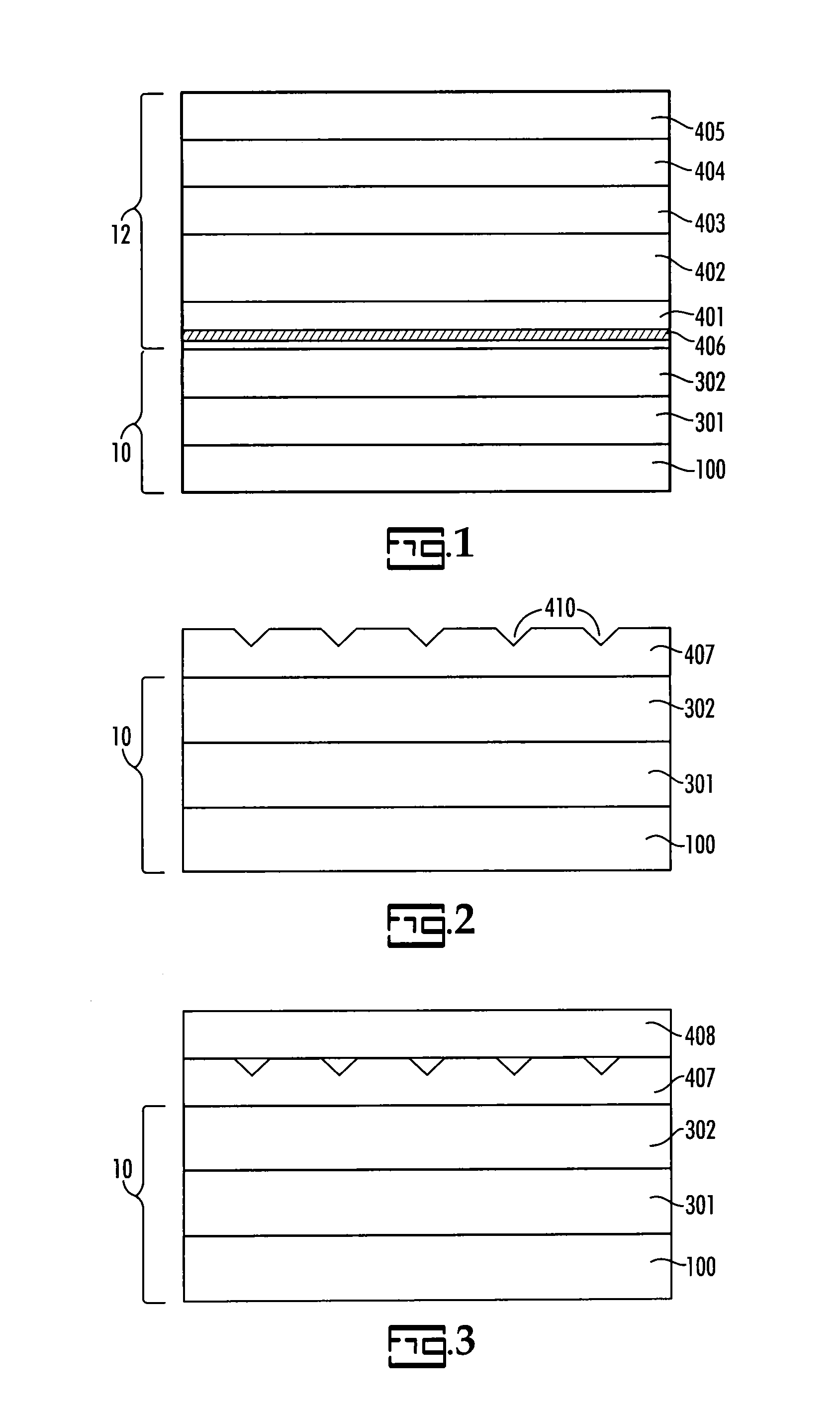
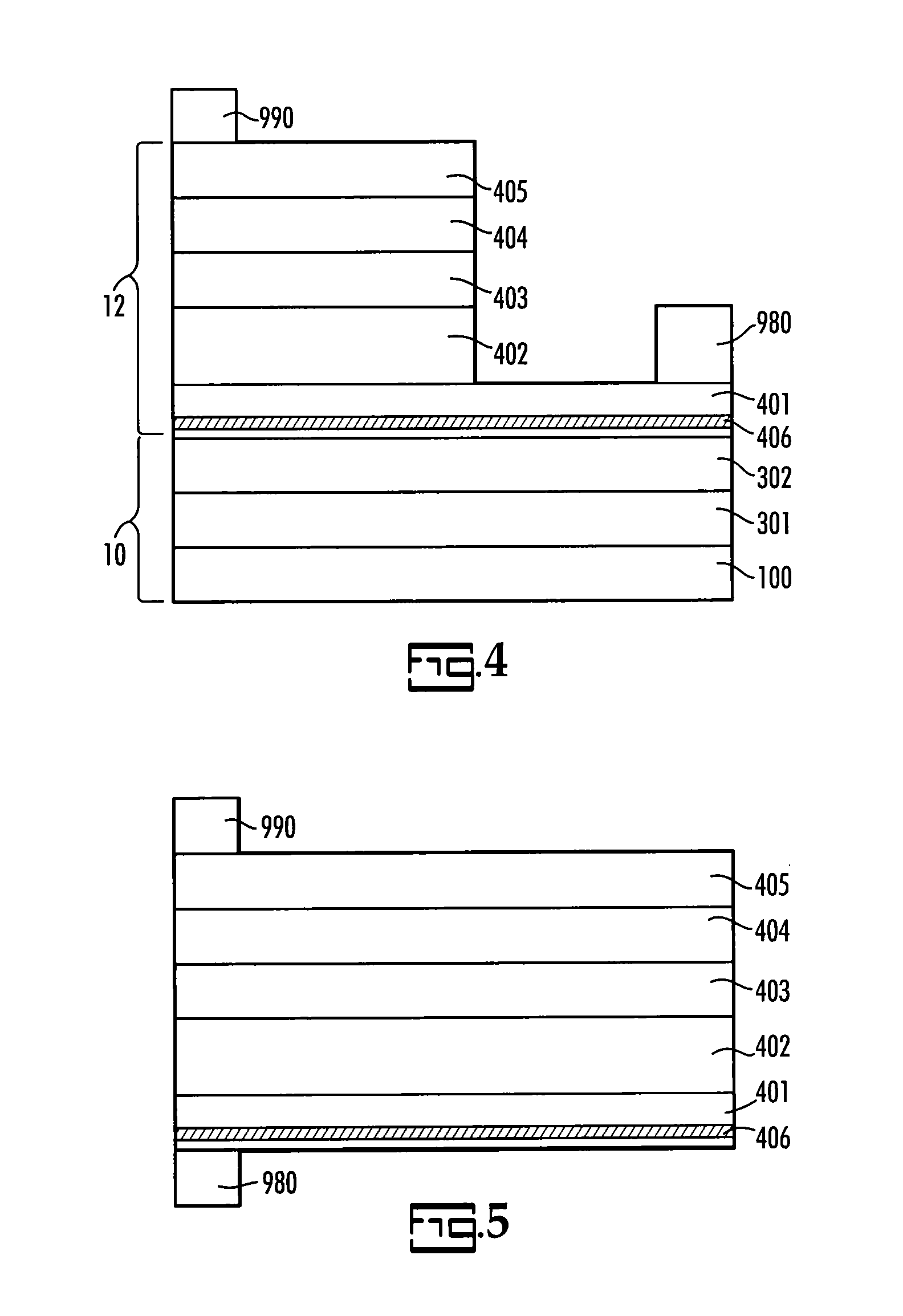
[0037]An embodiment of the invention will be described with reference to FIG. 1 wherein a schematic cross-sectional view is provided. In FIG. 1, a template, 10, includes a substrate, 100. A first buffer layer, 301, is added onto the substrate. A second buffer, 302, is applied to the first buffer. These buffer layers will be described more f...


PUM


Abstract

A low resistance light emitting device with an ultraviolet light-emitting structure having a first layer with a first conductivity, a second layer with a second conductivity; and a light emitting quantum well region between the first layer and second layer. A first electrical contact is in electrical connection with the first layer and a second electrical contact is in electrical connection with the second layer. A template serves as a platform for the light-emitting structure. The ultraviolet light-emitting structure has a first layer having a first portion and a second portion of AlXInYGa(1-X-Y)N with an amount of elemental indium, the first portion surface being treated with silicon and indium containing precursor sources, and a second layer. When an electrical potential is applied to the first layer and the second layer the device emits ultraviolet light.

Description

CROSS-REFERENCE TO RELATED APPLICATIONS[0001]The present invention claims priority to pending U.S. Provisional Patent Application No. 61 / 070,976 filed Mar. 27, 2008, and U.S. Provisional Patent No. 61 / 070,977 filed Mar. 27, 2008.BACKGROUND OF THE INVENTION[0002]The present invention relates generally to an ultraviolet light-emitting device and method of manufacturing a light-emitting device.[0003]Group III nitride compound semiconductors such as, for instance, gallium nitride (GaN), aluminum nitride (AlN), indium nitride (InN) (hereinafter also referred to as a “Group III-nitride semiconductor” or “III-nitrides”) have been gaining attention as a material for semiconductor devices that emit green, blue or ultraviolet light. A light-emitting diode or a laser diode that emits blue light may be used for displays, for lighting and for high-density optical disk devices. A light-emitting device (which together with the acronym LED, when used herein, will for convenience also refer to both ...

Claims


Application Information

Patent Timeline
Patent Type & Authority Patents(United States)
IPC IPC(8): H01L29/06H01L31/00H01L33/00H01L33/12H01L33/22H01L33/32
CPCH01L33/12H01L33/32H01L33/0079H01L33/22H01L33/0093
Inventor KHAN, ASIFFAREED, QHALIDADIVARAHAN, VINOD
Owner NIITEK
Why Eureka
Try Eureka