High-voltage BJT formed using CMOS HV processes

a high-voltage bipolar junction transistor and process technology, applied in the field of integrated circuits, can solve the problems of inefficient chip area usage of bjt, and achieve the effects of reducing chip area usage, increasing current gain, and reducing base resistan

Active Publication Date: 2013-04-09
TAIWAN SEMICON MFG CO LTD
View PDF6 Cites 63 Cited by
  • Summary
  • Abstract
  • Description
  • Claims
  • Application Information

AI Technical Summary

Benefits of technology

[0008]The advantageous features of the present invention include increased current gain, reduced chip area usage, and lower base resistance.

Problems solved by technology

In addition, the chip area usage of the BJT is not efficient.

Method used


Image

  • High-voltage BJT formed using CMOS HV processes
  • High-voltage BJT formed using CMOS HV processes
  • High-voltage BJT formed using CMOS HV processes

Examples


Embodiment Construction

[0013]The making and using of the embodiments of the present invention are discussed in detail below. It should be appreciated, however, that the embodiments provide many applicable inventive concepts that can be embodied in a wide variety of specific contexts. The specific embodiments discussed are merely illustrative of specific ways to make and use the invention, and do not limit the scope of the invention.

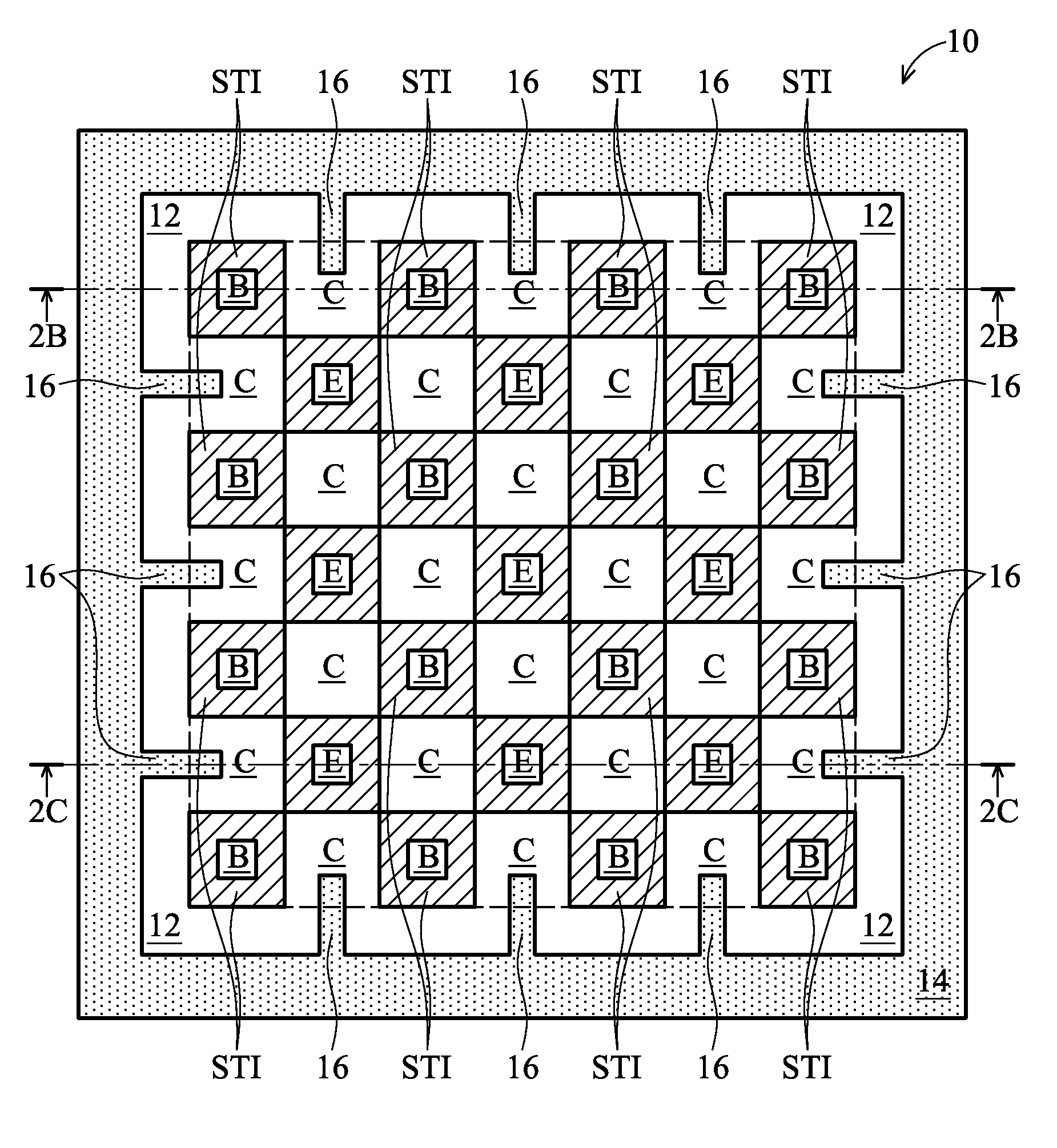
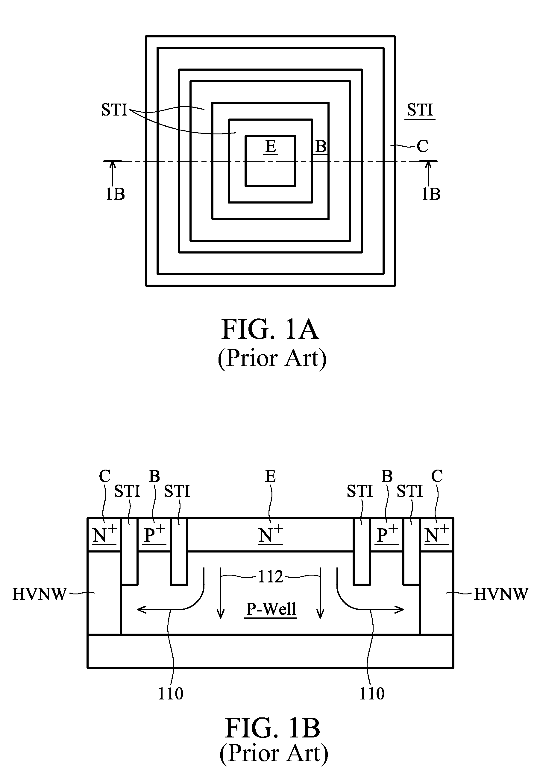
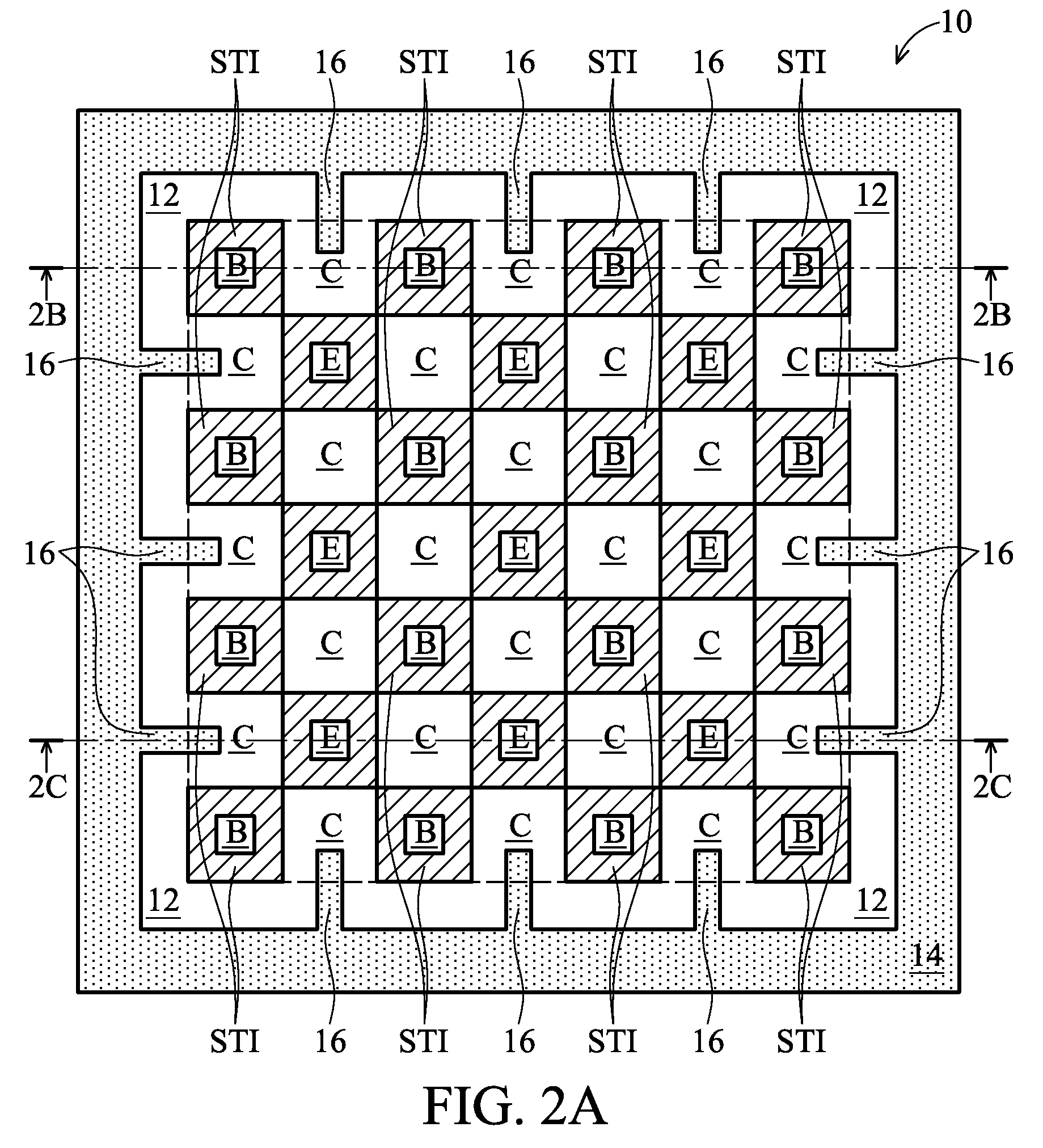
[0014]A novel high-voltage (HV) bipolar junction transistor (BJT) is provided. The variations and the operation of the embodiment are then discussed. Throughout the various views and illustrative embodiments of the present invention, like reference numbers are used to designate like elements. Throughout the description, NPN HVBJTs are discussed as exemplary embodiments. However, the teaching may also be applied to PNP HVBJTs, with the p-type and n-type regions inverted.

[0015]FIGS. 2A, 2B and 2C illustrate HVBJT 10 having a rectangular mash structure, which includes a plurality ...


PUM


Abstract

An integrated circuit device includes a semiconductor substrate having a top surface; at least one insulation region extending from the top surface into the semiconductor substrate; a plurality of base contacts of a first conductivity type electrically interconnected to each other; and a plurality of emitters and a plurality of collectors of a second conductivity type opposite the first conductivity type. Each of the plurality of emitters, the plurality of collectors, and the plurality of base contacts is laterally spaced apart from each other by the at least one insulation region. The integrated circuit device further includes a buried layer of the second conductivity type in the semiconductor substrate, wherein the buried layer has an upper surface adjoining bottom surfaces of the plurality of collectors.

Description

[0001]This application claims the benefit of U.S. Provisional Application No. 61 / 183,420 filed on Jun. 2, 2009, entitled “High-Voltage BJT Formed Using CMOS HV Processes,” which application is hereby incorporated herein by reference.TECHNICAL FIELD[0002]This invention relates generally to integrated circuits, and more particularly to high-voltage integrated circuits, and even more particularly to high-voltage bipolar junction transistors (BJTs) formed using standard high-voltage CMOS processes.BACKGROUND[0003]High-voltage devices are commonly used in integrated circuits, and may be used in input / output (IO) circuits, memory circuits, and the like. FIG. 1A illustrates a top view of a conventional high-voltage bipolar junction transistor (BJT). FIG. 1B illustrates a cross-sectional view of the structure as shown in FIG. 1A, wherein the cross-sectional view is taken along a plane crossing line 1B-1B. The BJT includes emitter E, collector C, and base contact B. Emitter E and collector C...

Claims


Application Information

Patent Timeline
Patent Type & Authority Patents(United States)
IPC IPC(8): H01L27/082
CPCH01L27/0823H01L29/0692H01L29/0821H01L29/7322H01L29/735
Inventor CHUNG, TAO-WENKE, PO-YAOLIN, WEI-YANGCHUNG, SHINE
Owner TAIWAN SEMICON MFG CO LTD
Why Eureka
Try Eureka