Active matrix substrate, liquid crystal panel, television receiver, method for producing liquid crystal panel

a liquid crystal panel and active matrix technology, applied in the field of active matrix substrate, liquid crystal panel, television receiver, method of producing liquid crystal panel, can solve the problem that the matrix substrate cannot correct the disconnection of the scanning signal line, and achieve the effect of improving the process yield

Active Publication Date: 2013-04-16
SHARP KK
View PDF20 Cites 0 Cited by
  • Summary
  • Abstract
  • Description
  • Claims
  • Application Information

AI Technical Summary

Benefits of technology

[0017]The active matrix substrate of the present invention can be configured to further include: electrodes for correction each electrically connected to a pixel electrode, the electrodes for correction each including an overlap section overlapping the storage capacitor line extended section or a conductive body electrically connected to the storage capacitor line extended section, the storage capacitor line extended section including a section that does not overlap the pixel electrode in a route from a point of connection with the storage capacitor line to the overlap section. When a bypass is formed as described above, a portion of the bypass overlaps a pixel electrode. This causes a capacitance (Cgd) between the pixel electrode and a scanning signal line to become higher than those of other pixel electrodes. In order to solve this problem, an electrode for correction and a storage capacitor electrode extended section are melt-connected in a case where a sub-pixel including the first pixel electrode becomes a bright dot due to an increase in this Cgd. This allows the pixel electrode (the pixel electrode overlapping the bypass) to be electrically connected to a main body of the storage capacitor line. This makes it possible to turn the sub-pixel including the first pixel electrode into a black dot.
[0019]The active matrix substrate of the present invention can also be configured such that: the each storage capacitor line extended section is formed along a pixel electrode. This makes it possible to shield an electric field produced by the data signal line, by use of the storage capacitor line extended section.
[0025]As described above, in the active matrix substrate of the present invention, a disconnection of a scanning signal line can be corrected. This makes it possible to improve a process yield in production of the active matrix substrate.

Problems solved by technology

However, the conventional active matrix substrate cannot correct a disconnection of a scanning signal line, which is a problem.

Method used


Image

  • Active matrix substrate, liquid crystal panel, television receiver, method for producing liquid crystal panel
  • Active matrix substrate, liquid crystal panel, television receiver, method for producing liquid crystal panel
  • Active matrix substrate, liquid crystal panel, television receiver, method for producing liquid crystal panel

Examples


embodiment 1

[0062][Embodiment 1]

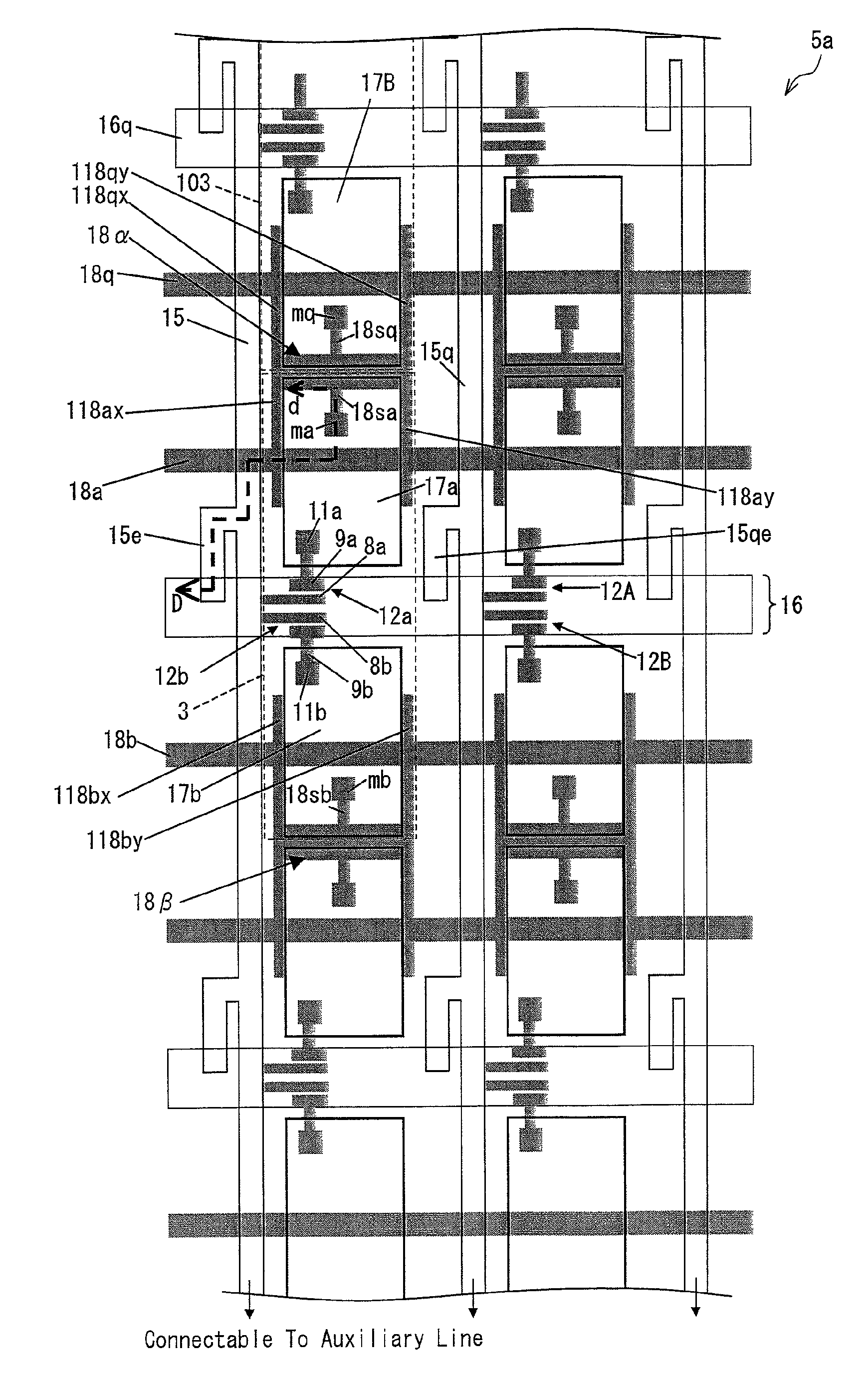
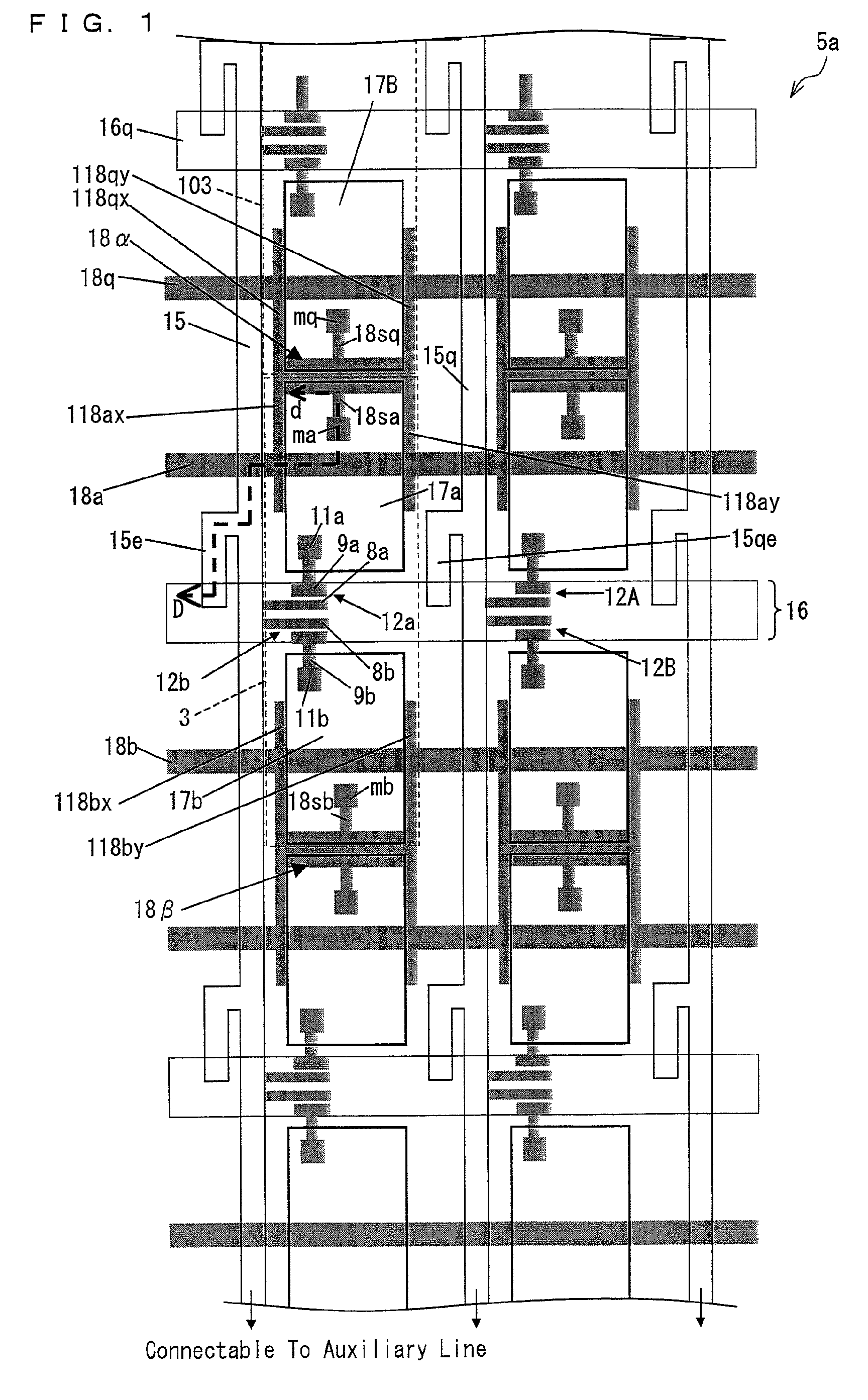
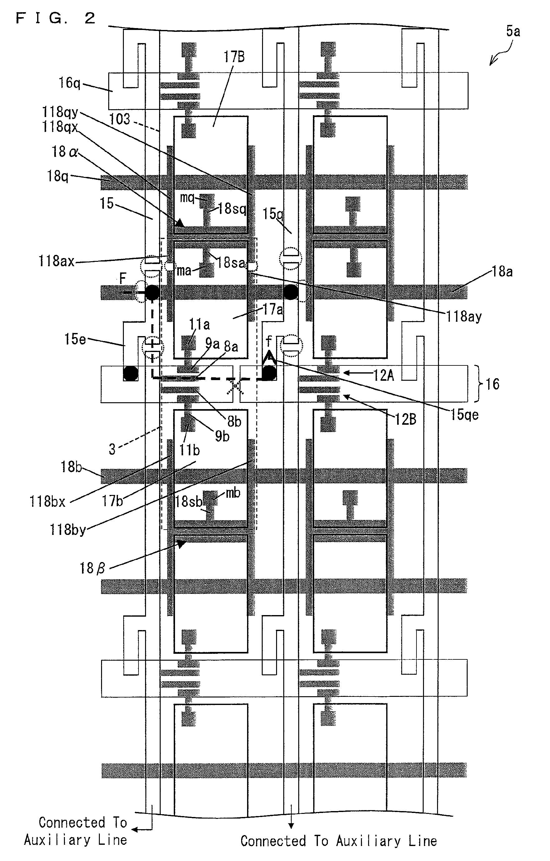
[0063]FIG. 1 illustrates a configuration of an active matrix substrate of the present embodiment. The active matrix substrate of the present embodiment in FIG. 1 is an active matrix substrate 5a in a pixel division system. As shown in FIG. 1, this active matrix substrate 5a includes data signal lines (15, 15q) extending in a column direction, scanning signal lines (16, 16a) extending in a row direction, and storage capacitor lines (18a, 18b, 18q) extending in the row direction. In this active matrix substrate 5a, pixel areas 3 are provided in a matrix form. Each of the data signal lines intersects with the storage capacitor lines and the scanning signal lines.

[0064]The scanning signal line 16 crosses a center of corresponding pixel areas 3. In a pixel area 3, first and second transistors 12a and 12b and first and second pixel electrodes 17a and 17b are formed. It should be noted that, when viewed in plane, the first pixel electrode 17a and the first storage capac...

embodiment 2

[0104][Embodiment 2]

[0105]An active matrix substrate of the present embodiment, that is, an active matrix substrate 5d can be configured as shown in FIG. 8. The active matrix substrate 5d has a configuration that makes it possible to correct a scanning signal line by using no auxiliary line. In the active matrix substrate 5d, a data signal line extended section extends from a position on a data signal line between (i) an intersection of the data signal line and one of two adjacent scanning signal lines and (ii) an intersection of the data signal line and the other one of the two adjacent scanning signal lines. One of two storage capacitor lines adjacent to a scanning signal line which the data signal line extended section overlaps is defined as an adjacent storage capacitor line. Further, out of two scanning signal lines adjacent to the scanning signal line which the data signal line extended section overlaps, one scanning signal line provided on the same side as the adjacent storag...


PUM

PropertyMeasurementUnit
wavelengthaaaaaaaaaa
areaaaaaaaaaaa
areasaaaaaaaaaa

Abstract

An active matrix substrate includes: storage capacitor line extended sections 118ax, 118qx, etc. each extending from a position on a storage capacitor line between (i) an intersection with one of two adjacent data signal lines 15 and 15q and (ii) an intersection with the other one of the two data signal lines 15 and 15q; and data signal line extended sections 15e and 15qe each extending from a position on a data signal line 15 or 15q between (i) an intersection with one of two adjacent scanning signal lines 16 and 16q and (ii) an intersection with the other one of the two adjacent scanning signal lines 16 and 16q, wherein a storage capacitor line extended section 118ax or 118ay extending from one of two adjacent storage capacitor lines 18a and 18q sandwiching no scanning signal line is connected with a storage capacitor line extended section 118qx or 118qy extending from the other one of the two adjacent storage capacitor lines 18a and 18q, wherein each of the storage capacitor line extended sections 118ax, 118ay, 118qz, and 118qy includes a section that does not overlap a pixel electrode, wherein each of the data signal line extended sections 118ax, 118ay, 118qz, and 118qy has a section overlapping a scanning signal line. This configuration makes it possible to correct a disconnection of a scanning signal line in an active matrix substrate.

Description

TECHNICAL FIELD[0001]The present invention relates to an active matrix substrate capable of correcting a disconnection of a scanning signal line, and a liquid crystal panel using the active matrix substrate.BACKGROUND ART[0002]FIG. 17 shows a conventional configuration of an active matrix substrate (of a pixel division system) that has a multi-pixel structure. As shown in FIG. 17, an active matrix substrate 905 includes data signal lines 915 extending in a column direction, scanning signal lines 916 extending in a row direction, storage capacitor lines 918a and 918b extending in the row direction, and pixel areas 903 partitioned by the data signal lines and the storage capacitor lines. Each scanning signal line 916 crosses a center of corresponding pixel areas 903. In each pixel area 903, first and second transistors 912a and 912b, and first and second pixel electrodes 917a and 917b are formed. Note that one storage capacitor line (918a or 918b) is provided so as to correspond to tw...

Claims


Application Information

Patent Timeline
Patent Type & Authority Patents(United States)
IPC IPC(8): G02F1/1343G02F1/136
CPCG02F1/136213H01L27/1255G02F1/136259G02F2001/136263G02F1/136263
Inventor SHOHRAKU, AKIHIRO
Owner SHARP KK
Why Eureka
Try Eureka