Methods of patterning a conductor on a substrate

a technology of conductor and substrate, which is applied in the direction of circuit mask, instrument, photomechanical apparatus, etc., can solve the problems of inability to displace the incumbent process commercially, impede the commercialization of microcontact printing in the etch-patterning of metals, and inacceptable pattern distortion and artifacts

Inactive Publication Date: 2013-04-23
3M INNOVATIVE PROPERTIES CO
View PDF57 Cites 14 Cited by
  • Summary
  • Abstract
  • Description
  • Claims
  • Application Information

AI Technical Summary

Problems solved by technology

At the same time, there are many other unique methods that to date have failed to displace the incumbent processes commercially, for example due to lack of a true advantage or due to significant technical barriers to implementation.
Significant technical barriers have impeded the commercialization of microcontact printing in the etch-patterning of metals.
Notwithstanding these features, the method has been revealed through extensive research to pose significant challenges related to pattern geometry flexibility and to scale-up.
For example, in the art it is known that microcontact printing patterns with widely spaced features leads to stamp deformation, including roof collapse, which leads to unacceptable pattern distortion and artifacts.
These issues have led to the engineering of composite stamps with complicated constructions, usually comprising very stiff or very thin layers of the elastomer stamp material, or sometimes including mounting of the stamp on supports or backplanes with specified properties.
In other approaches, stamps with significant relief have been proposed, leading to challenges in mastering and printing.
Often, the material changes or stamp construction or support measures lead to challenges in generating an inked stamp that can be used to print patterns efficiently, for example with high throughput and at competitive cost.
The convolution of these kinetic factors makes the ability, let alone the sufficient optimization for commercialization, of microcontact printing to generate any particular pattern uncertain.
Another important challenge in microcontact printing relates to printing features of different scale simultaneously.
Owing to the aforementioned (but not entirely understood) kinetic factors, it is unknown whether particular combinations of features sizes and spacings can be printed effectively and with useful speeds.
No obvious and practical condition exists for printing alkanethiols to form both small and large features at the same time while maintaining the accuracy of the former.
Another important but unpredictable factor that influences whether a particular metal pattern can be successfully generated under a given set of printing and etching conditions is the surface onto which the SAM is printed, for example as determined by a substrate onto which the metal is deposited.

Method used


Image

  • Methods of patterning a conductor on a substrate
  • Methods of patterning a conductor on a substrate
  • Methods of patterning a conductor on a substrate

Examples


example 1

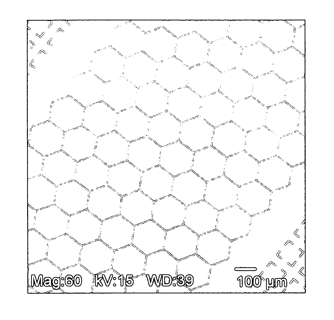
[0091]An electrically conductive micropattern (V1) of thin film silver was fabricated and characterized according to the procedures described above. The ink solution comprised hexadecylthiol dissolved in ethanol at a concentration of 10 mM. The ink solution was contacted to the back side of the stamp for 2.3 hours, leading to a hexadecylthiol concentration in the PDMS adjacent to the printing or stamping surface of approximately 0.8 mM. The stamping time was 10 seconds and there was an applied mass of 260 g during stamping. FIG. 11 gives an SEM photomicrograph recorded from the completed thin film metal micropattern, derived from a low-density region comprising a hexagonal mesh with 97% open area and target trace width of 3 μm. The actual trace width measured over 5 μm.

example 2

[0092]An electrically conductive micropattern (V2) of thin film silver was fabricated and characterized according to the procedures described above. The ink solution comprised hexadecylthiol dissolved in ethanol at a concentration of 10 mM. The ink solution was contacted to the back side of the stamp for 17.5 hours, leading to a hexadecylthiol concentration in the PDMS adjacent to the printing or stamping surface of approximately 5 mM. The stamping time was 5 seconds and there was no mass applied to the substate-stamp assembly after rolling application of the substrate to the stamp. FIGS. 8, 9, and 10 give SEM photomicrographs recorded from the completed thin film metal micropattern. FIG. 12 is another SEM photomicrograph of the completed thin film silver micropattern, derived from a low-density region comprising a hexagonal mesh with 97% open area and target trace width of 3 μm. The actual trace width measured approximately 3.2 μm.

examples 3-42

[0093]Electrically conductive micropatterns of thin film silver were fabricated according to the process parameters listed in Table 1. Tables 2-7 give the quality factors assigned to selected examples, per the descriptions of quality factors given above. Examples that are not represented in Tables 2-7 are Examples 3, 4, 23 and 24, for which the stamping and etching steps yielded a very poorly defined pattern. For Example 38, a low density mesh region (square grid with 5 μm wide traces and 10% fill factor) of the conductor micropattern, measuring 1 mm in width and 33 mm in length and terminated at each end with a 2 mm by 2 mm pad, exhibited a resistance of 229 ohms. The resistance reading corresponds to a sheet resistance for the visible light transparent mesh region of 229 / 33=7 ohms per square. For Example 38, a low density mesh region (square grid with 3 μm wide traces and 5% fill factor) of the conductor micropattern, measuring 1 mm in width and 33 mm in length and terminated at e...


PUM

PropertyMeasurementUnit
widthaaaaaaaaaa
distanceaaaaaaaaaa
widthaaaaaaaaaa

Abstract

A method of patterning a conductor on a substrate includes providing an inked elastomeric stamp inked with self-assembled monolayer-forming molecules and having a relief pattern with raised features. Then the raised features of the inked stamp contact a metal-coated visible light transparent substrate. Then the metal is etched to form an electrically conductive micropattern corresponding to the raised features of the inked stamp on the visible light transparent substrate.

Description

CROSS REFERENCE TO RELATED APPLICATIONS[0001]This application claims the benefit of U.S. Provisional Patent Application 61 / 032,273 filed on Feb. 28, 2008, which is hereby incorporated by reference in its entirety.BACKGROUND[0002]There are numerous methods for patterning metals on surfaces, many of which are widely practiced commercially, including for example photolithography with etching or with plating, inkjet printing, screen-printing, and laser patterning. At the same time, there are many other unique methods that to date have failed to displace the incumbent processes commercially, for example due to lack of a true advantage or due to significant technical barriers to implementation. Significant technical barriers have impeded the commercialization of microcontact printing in the etch-patterning of metals.[0003]Microcontact printing is the stamping or rotary printing of self-assembled monolayer (SAM) patterns on substrate surfaces. The approach exhibits several technologically ...

Claims


Application Information

Patent Timeline
Patent Type & Authority Patents(United States)
IPC IPC(8): B44C1/22
CPCB82Y10/00B82Y40/00G03F7/0002G06F3/044G06F3/041H05K3/061B41M5/52H05K3/0079G06F2203/04103G06F2203/04112H05K2201/0108H05K2201/0133H05K2203/0108H05K2203/0537C23F1/02C23F1/30Y10T428/24802G06F3/0445H05K1/0296H05K1/032
Inventor ZU, LIJUNFREY, MATTHEW H.
Owner 3M INNOVATIVE PROPERTIES CO
Why Eureka
Try Eureka