
Organic photoactive device

a photoactive device and organic technology, applied in the field of organic photoactive devices, can solve the problems of maximizing the open-circuit photovoltage of the device, unable to achieve typical efficiencies of 10% to 20% such as are known for inorganic solar cells, and achieve the effect of improving yield

Active Publication Date: 2013-04-23
HELIATEK GMBH +1
View PDF41 Cites 30 Cited by
  • Summary
  • Abstract
  • Description
  • Claims
  • Application Information

AI Technical Summary

Benefits of technology

The invention aims to improve the yield of an organic photoactive device, specifically an inorganic photovoltaic cell.

Problems solved by technology

In this manner previously typical efficiencies of 10% to 20% such as are known for inorganic solar cells have not yet been able to be achieved.
The latter results in a maximizing of the open circuit photovoltage of the device.

Method used


Image

  • Organic photoactive device
  • Organic photoactive device
  • Organic photoactive device

Examples


example 1

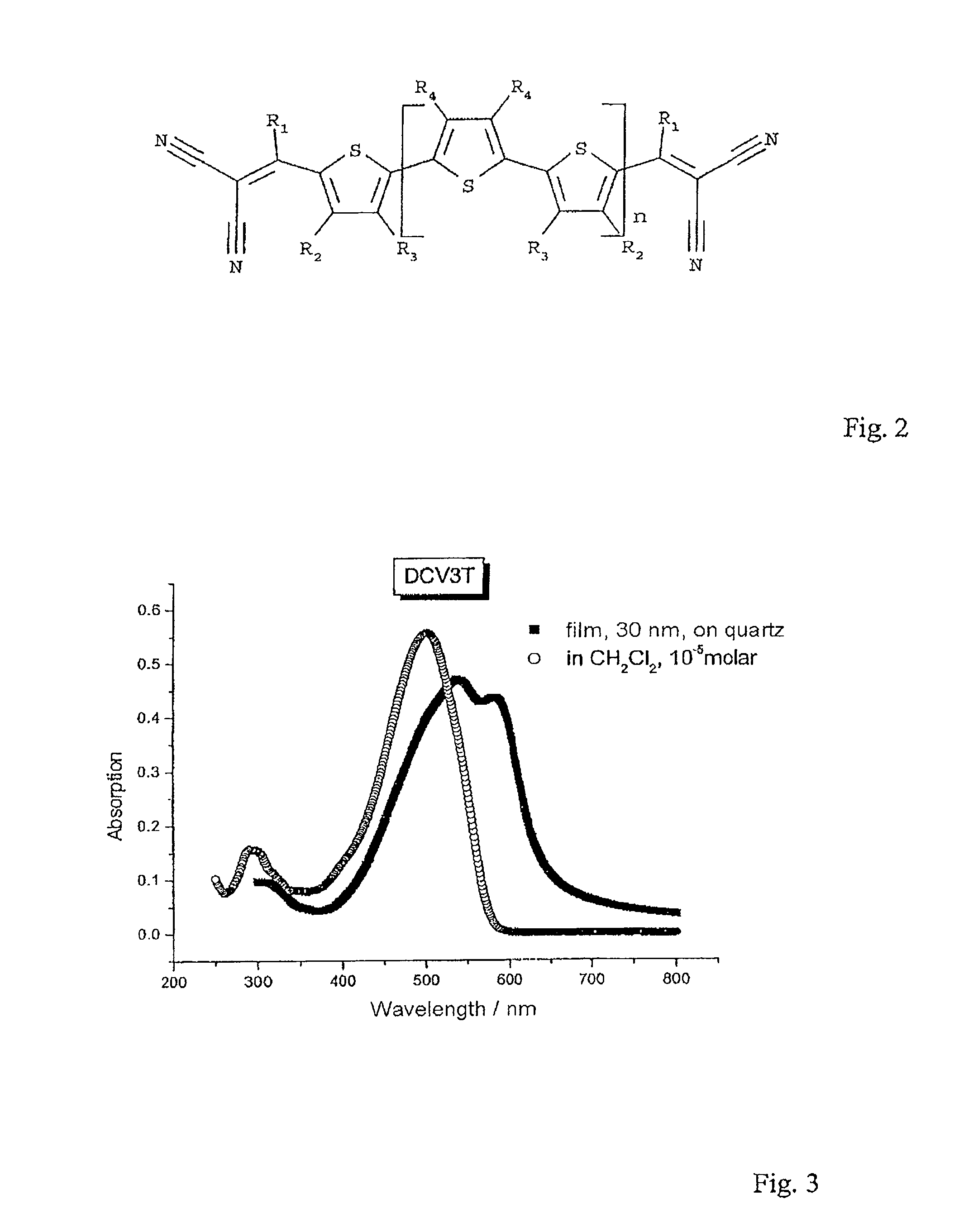
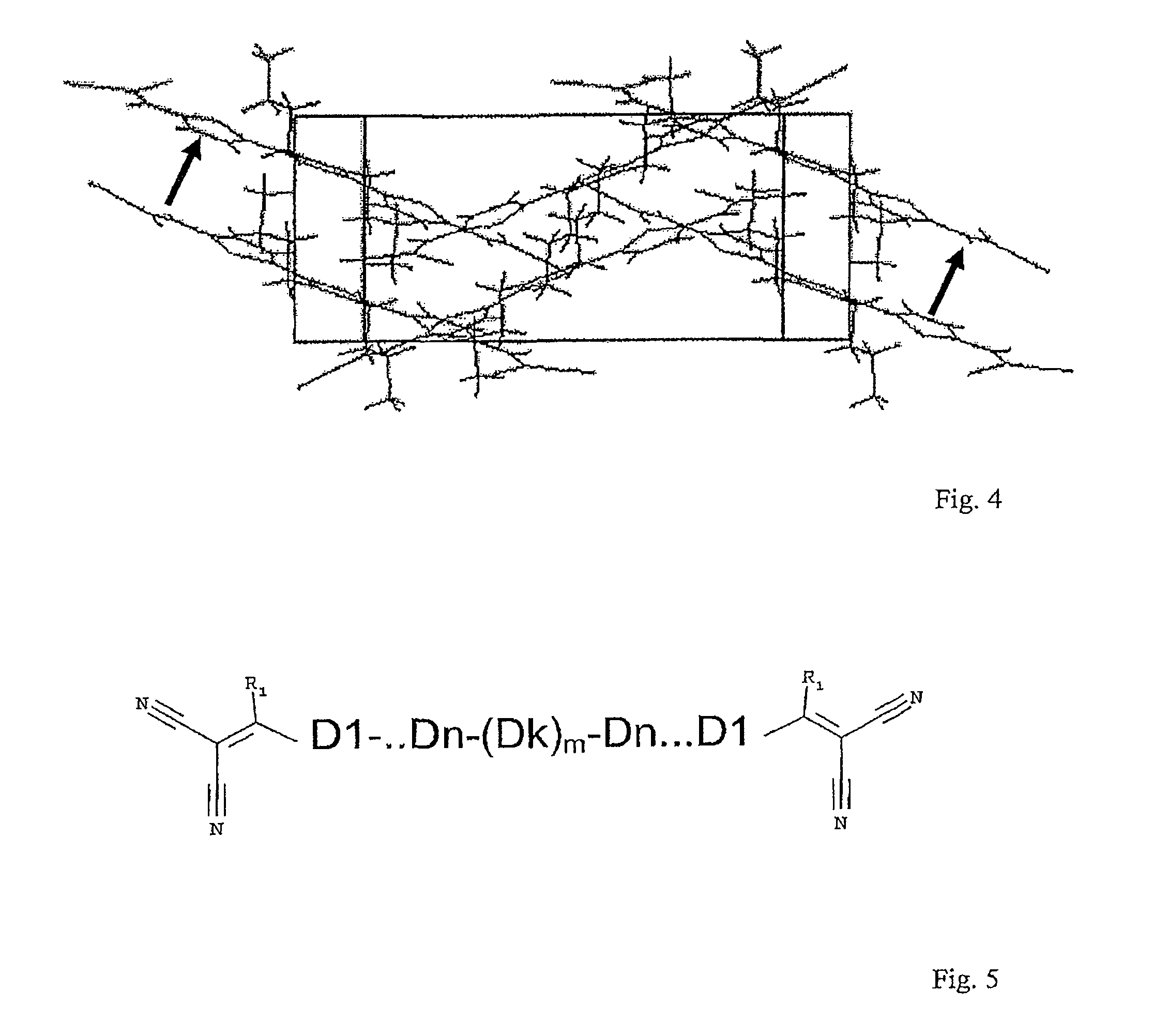
[0122]In a first example DCV3T (cf. structure in FIG. 5 with n=1 and group R1=hydrogen atom) is used as acceptor molecule in a heterojunction with N,N,N′,N′-tetrakis(4-methoxyphenyl) benzidine (MeOTPD) as donor molecule. A possible layer sequence for such a heterojunction, inserted into an M-i-p structure, is: Glass substrate / ITO / C60 (optional as electron transport layer) / DCV3T / MeOTPD / p-doped MeOTPD / p-doped zinc phthalocyanine (ZnPc; optional for improving the ohmic contact) / gold.

[0123]Since MeOTPD is largely transparent and the interface between C60 and DCV3T is not suitable for exciton separation, the generation of photocurrent results here exclusively from the light absorption in DCV3T and the subsequent exciton separation on the interface between DCV3T and MeOTPD.

[0124]FIG. 14 shows a current-voltage characteristics with illumination for a solar cell with a 20 nm-thick DCV3T layer and a 5 nm-thick layer of pure MeOTPD that make the exciton-separating interface available. The pre...

example 2

[0125]In a second example the transparent MeOTPD in example 1 is replaced at the top by a layer of ZnPc, so that the layer sequence is: Glass substrate / ITO / C60 (optional as electron transport layer) / DCV3T / ZnPc / p-doped MeOTPD / p-doped ZnPc (optional for improving the ohmic contact) / gold.

[0126]FIG. 15 shows a current-voltage characteristics with and without illumination for a solar cell with a 20 nm-thick DCV3T layer and a 10 nm-thick ZnPc layer. These layers form the separating interface for excitons. The precise layer sequence and the characteristic parameters of the illuminated solar cell are also indicated in FIG. 14.

[0127]The functional principle corresponds to that in example 1 above. In addition, a generation of photocurrent takes place by light absorption on ZnPc and exciton separation on the heterojunction to DCV3T. As a result, the short-circuit current (jsc) is enlarged in comparison to example 1 above.

[0128]In examples 1 and 2 the A-D-A′-BCO DCV3T is therefore used as accep...

example 3

[0130]In a third example the DCV3T from example 1 is replaced by DCV5T (cf. structure in (FIG. 5) with n=2 and R1=hydrogen) for further increasing the light absorption in the red spectral range so that the following layer sequence results: Glass substrate / ITO / C60 / DCV5T / MeOTPD / p-doped MeOTPD / p-doped ZnPc (optional for improving the ohmic contact) / gold.

[0131]It was found that in the third example, in contrast to examples 1 and 2, the photoactive interface occurs between DCV5T and C60, the A-D-A′-BCO DCV5T acting, in contrast to DCV3T, as donor in the photoactive heterojunction and as hole conductor. The difference is explained by the lower ionization energy of the DCV5T molecule, which has the longer donor block.

[0132]FIG. 16 shows a current-voltage characteristics with and without illumination for a solar cell with a 20 nm-thick C60 layer and a 15 nm-thick DCV5T layer that act here as active materials. The layer sequence is indicated in the insert. The cell achieves an open circuit v...


PUM

PropertyMeasurementUnit
HOMOaaaaaaaaaa
LUMOaaaaaaaaaa
optical absorption coefficientsaaaaaaaaaa

Abstract

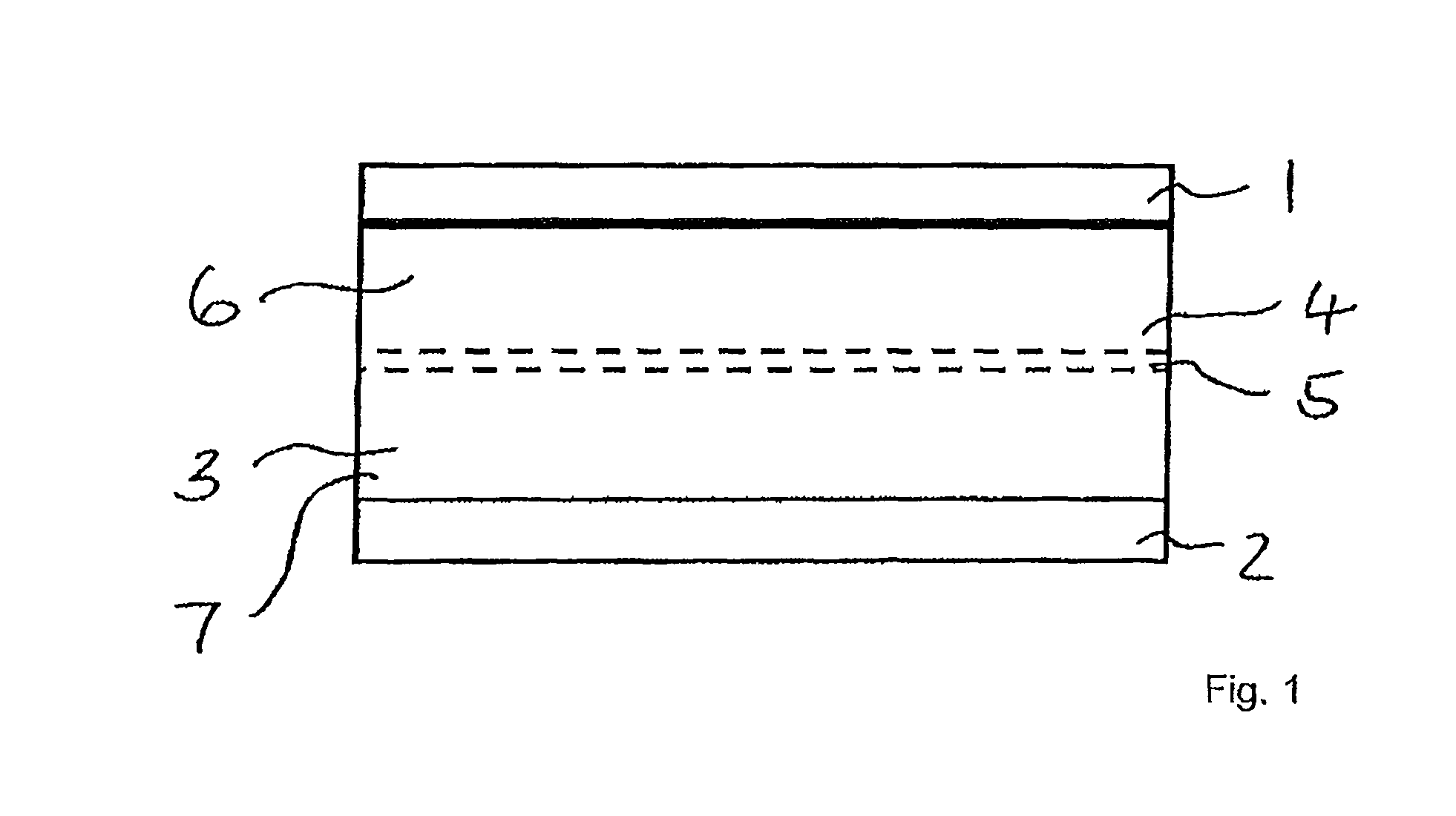
The invention relates to an organic photoactive device, especially an organic photovoltaic cell, with a contact and a countercontact as well as with an organic region that is electrically connected to the contact and the countercontact, wherein a photoactive region with a photoactive bulk heterojunction or a flat heterojunction between an electron-conducting organic material and a hole-conducting organic material is formed in the organic region and wherein the hole-conducting organic material and / or the electron-conducting organic material is formed from oligomers according to any one of the following types: conjugated acceptor-donor-acceptor oligomer (A-D-A′ oligomer) with an acceptor unit (A) and a further acceptor unit (A′) that are each connected to a donor unit (D), and conjugated donor-acceptor-donor oligomer (D-A-D′ oligomer) with a donor unit (D) and a further donor unit (D′) that are each connected to an acceptor unit (A).

Description

CROSS-REFERENCE TO RELATED APPLICATIONS[0001]The present application is a 35 U.S.C. §§371 national phase conversion of PCT / DE2006 / 000394, filed Mar. 3, 2006, which claims priority of German Patent Application No. 10 2005 010 978.0, filed Mar. 4, 2005, which are herein incorporated by reference. The PCT International Application was published in the German Language.[0002]The invention relates to an organic photoactive device, especially an organic photovoltaic cell, with a contact and a countercontact as well as with an organic region that is electrically connected to the contact and the countercontact, wherein a photoactive region is formed with a photoactive heterojunction between an electron-conducting organic material and a hole-conducting organic material in the organic region.BACKGROUND OF THE INVENTION[0003]The research and development in the region of organic photoactive devices, formed in a known embodiment as an organic solar cell or organic photovoltaic cell, has sharply i...

Claims


Application Information

Patent Timeline
Patent Type & Authority Patents(United States)
IPC IPC(8): H01L31/00
CPCB82Y10/00H01L51/0036H01L51/0068H01L51/4246H01L51/4253H01L51/0046H01L51/0051H01L51/0059H01L51/0077Y02E10/52Y02E10/549Y02P70/50H10K85/211H10K85/113H10K85/611H10K85/655H10K85/631H10K85/30H10K30/211H10K30/30H10K30/50
Inventor PFEIFFER, MARTINUHRICH, CHRISTIANPETRICH, ANNETTESCHUPPEL, RICOSCHULZE, KERSTINLEO, KARLBAUERLE, PETERREINOLD, EGONBRIER, EDUARD
Owner HELIATEK GMBH
Learn More