Electrically isolated power semiconductor package with optimized layout

a technology of power semiconductor and optimized layout, which is applied in the direction of semiconductor devices, semiconductor device details, semiconductor/solid-state devices, etc., can solve the problems of power semiconductor devices being exposed, other circuit components, and safety hazards for operating personnel

Active Publication Date: 2013-06-04
LITTELFUSE INC
View PDF3 Cites 40 Cited by
  • Summary
  • Abstract
  • Description
  • Claims
  • Application Information

AI Technical Summary

Problems solved by technology

Additionally, the power semiconductor device may be exposed to voltages outside of the intended range during operation, which may electrically couple to the backside of the package.
The high voltages present at the backside of conventional packaged power semiconductor devices may damage other circuit components or may present a safety hazard to operating personnel or to operating equipment built with these devices.
Voltages as low as 40 V can be a hazard to operators working with such equipment.
However, the heatsink 14 would typically need to be isolated from the rest of the circuit or chassis, and may require a shield to prevent a technician from inadvertently touching an electrically “hot” heatsink, which could be at a lethal voltage.

Method used


Image

  • Electrically isolated power semiconductor package with optimized layout
  • Electrically isolated power semiconductor package with optimized layout
  • Electrically isolated power semiconductor package with optimized layout

Examples


Embodiment Construction

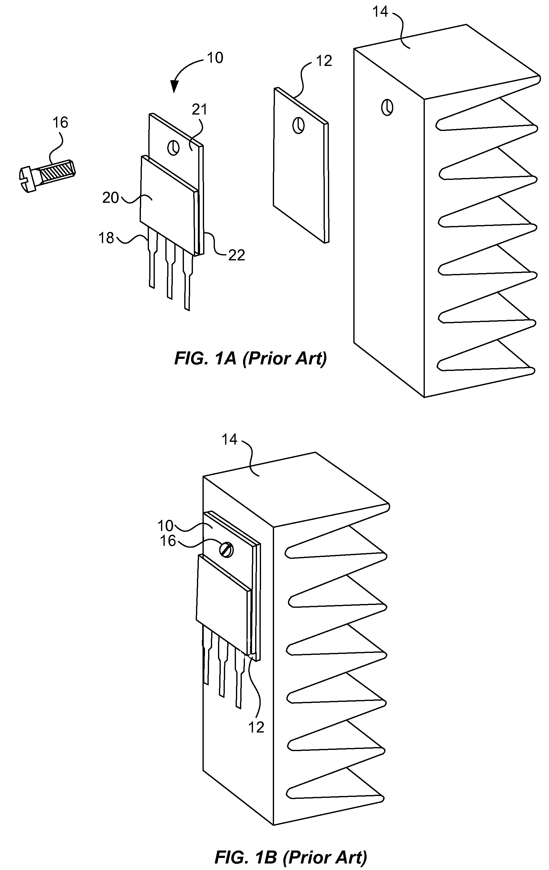
[0037]The present invention provides a packaged power semiconductor device with superior safety, performance, manufacturability, and attachment capabilities.

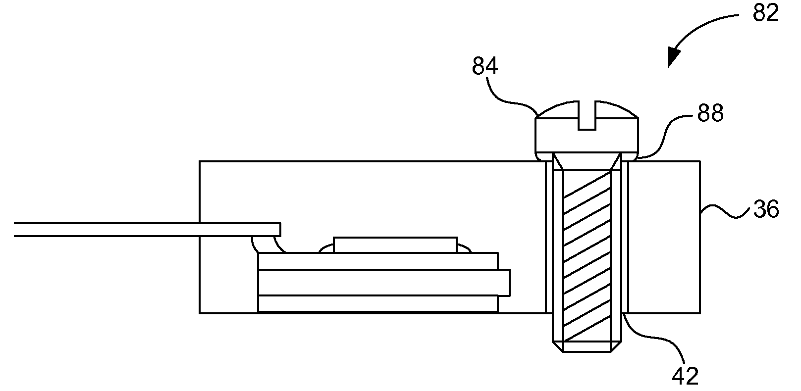
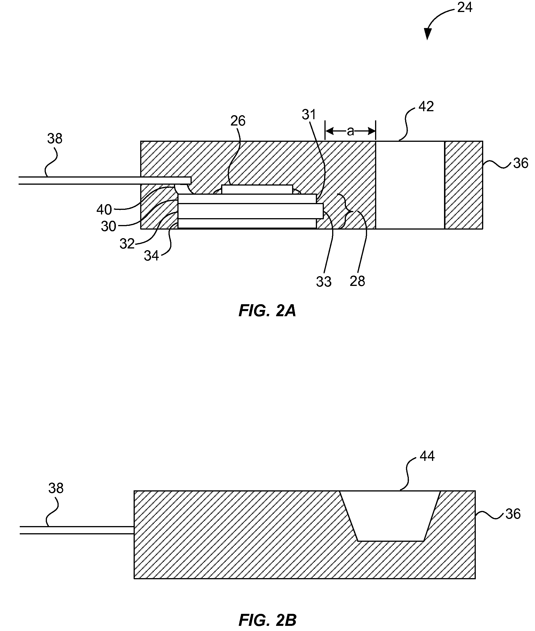
[0038]FIG. 2A shows a simplified cross section of a packaged power semiconductor device 24 according to one embodiment of the present invention. A power semiconductor die 26 is soldered to a direct bonded copper (“DBC”, also known as direct copper bonded (“DCB”)) substrate 28. The DBC substrate 28 includes a die-side (first) layer of copper 30, a layer of ceramic 32, and a back-side (second) layer of copper 34. A layer of encapsulant 36 is formed over the power semiconductor die 26, the DBC substrate 28, and device leads 38 (only one of which is shown). The device leads 38 may be used for electrically accessing the power semiconductor die 26, and may be electrically coupled to various portions of the packaged power semiconductor device. A center lead 38, as shown in the figure, includes a bent portion 40 and is soldered to the d...


PUM


Abstract

A packaged power semiconductor device is provided with voltage isolation between a metal backside and terminals of the device. The packaged power semiconductor device is arranged in an encapsulant defining a hole for receiving a structure for physically coupling the device to an object. A direct-bonded copper (“DBC”) substrate is used to provide electrical isolation and improved thermal transfer from the device to a heatsink. At least one power semiconductor die is mounted to a first metal layer of the DBC substrate. The first metal layer spreads heat generated by the semiconductor die. In one embodiment, the packaged power semiconductor device conforms to a TO-247 outline and is capable of receiving a screw for physically coupling the device to a heatsink.

Description

CROSS-REFERENCES TO RELATED APPLICATIONS[0001]The present application claims priority to U.S. Provisional Patent Application No. 61 / 187,537, filed on Jun. 16, 2009, which is incorporated by reference in its entirety.TECHNICAL FIELD[0002]This invention relates to electronic devices, and more particularly to a packaged power semiconductor device having an optimized layout for facilitating electrical isolation, thermal coupling and screw mounting, where the device includes a metal back plane that is electrically isolated from the terminals of the device.BACKGROUND OF THE INVENTION[0003]Most power semiconductor devices like silicon-controlled rectifiers (“SCRs”), power transistors, insulated gate-bipolar transistors (“IGBTs”), metal-oxide-semiconductor field effect transistors (“MOSFETs”), power rectifiers, power regulators, or combinations thereof, are assembled in packages that fail to provide sufficient electrical isolation. That is, a metal tab, which typically forms the backside of...

Claims


Application Information

Patent Timeline
Patent Type & Authority Patents(United States)
IPC IPC(8): H01L23/02
CPCH01L21/56H01L23/3735H01L23/4006H01L23/49541H01L21/52H01L23/3157H01L23/4334H01L23/49562H01L23/49575H01L23/3107H01L24/97H01L2924/1305H01L2924/13034H01L2924/1306H01L2023/4031H01L2023/4087H01L2023/405H01L2924/3025H01L2924/19107H01L2224/48091H01L21/565H01L2924/13055H01L2924/13091H01L2924/00014H01L2924/00H01L2224/49113H01L2924/15747H01L2924/15787H01L2924/181H01L2224/0603H01L2924/00012
Inventor SPANN, THOMASOSTMANN, HOLGERCHOI, KANG RIM
Owner LITTELFUSE INC
Why Eureka
Try Eureka