

Start-up procedure for an isolated switched mode power supply
- Summary
- Abstract
- Description
- Claims
- Application Information
AI Technical Summary
Benefits of technology
Problems solved by technology
Method used
Image

Examples
first embodiment
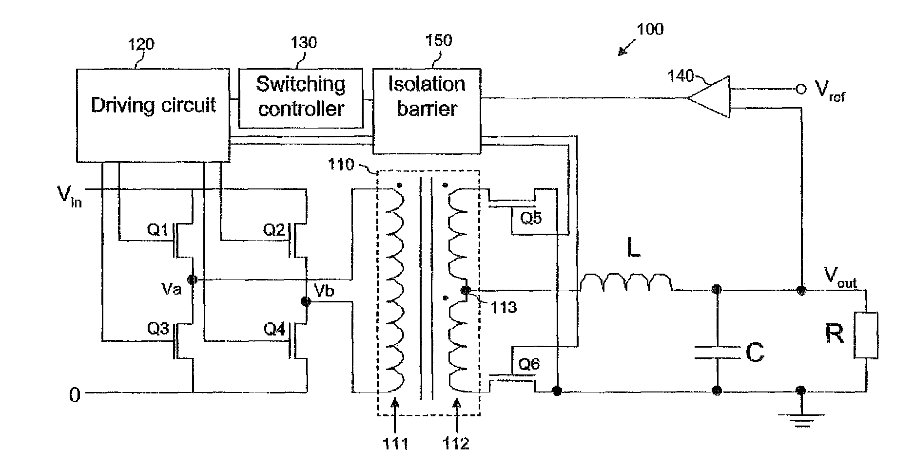
[0047]An isolated SMPS 200 according to first embodiment of the present invention is illustrated in FIG. 1. The SMPS 200 differs from the background example of FIG. 1 by the configuration of the switching controller 230.
[0048]In particular, the switching controller 230 of the present embodiment is operable to start up the isolated SMPS 200 from an inoperative state by generating start-up switching control signals during start-up of the SMPS 200, and operational switching control signals of period T during subsequent operation of the isolated SMPS 200 in its normal operational mode. In other words, the switching controller 230 is operable control the operation of the SMPS 200 with a set of start-up switching control signals whilst operating in a start-up mode, and with operational switching control signals of period T during subsequent operation of the switching controller 230 in the normal operation mode. In the normal operational mode, the switching controller 230 of the present em...
second embodiment
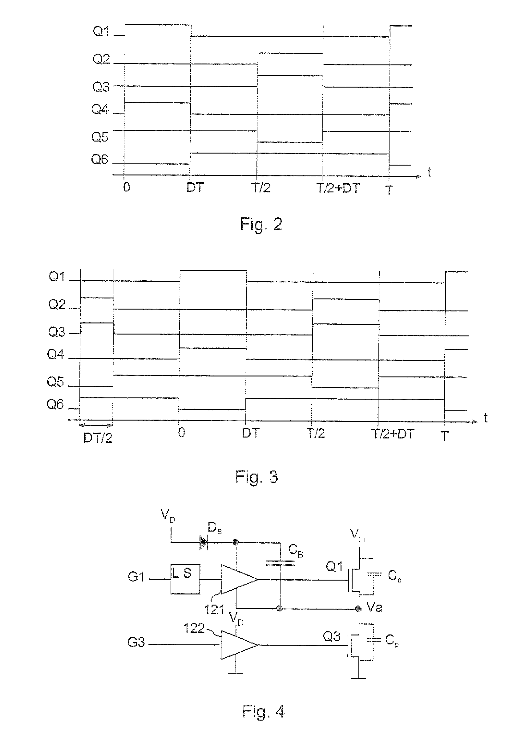
[0055]In the above-described first embodiment the start-up switching control signals shown in FIG. 6, and the above-mentioned variant of this timing diagram, both have the drawback that the parasitic capacitance of the transistor Q3 (or, as the case may be, Q4) that is not switched by the first pulse is discharged through transformer 110, causing a small imbalance in the isolation transformer flux.
[0056]However, in the second embodiment of the present invention, the charging of the boot-strap capacitors CB in the boot-strap circuits of both high-side transistors Q1 and Q2 is performed by switching ON both Q3 and Q4 with the first voltage pulse applied to each of these transistors. At the same time, both of the parasitic capacitances of these low-side transistors Q3 and Q4 are discharged, which improves the accuracy of the reduced-pulse transformer balancing. Then, within the same switching period T, transistors Q2 and Q3 are switched ON, each by the second voltage pulse which is gen...
third embodiment
[0057]In the third embodiment of the present invention, in order to minimize the number of PWM signals generated by the switching controller 230, transistors Q1 and Q4 are both controlled by a first PWM signal, and transistors Q2 and Q3 are both be controlled by a second PWM signal. In this case, the full start-up timing diagram takes the form shown in FIG. 8.
[0058]As shown in FIG. 8, the switching controller 230 starts up the SMPS 200 by generating a first voltage pulse of duration P1 for each of transistors Q1 and Q4 to temporarily switch them ON, and a subsequent second voltage pulse of duration P2 (preferably equal to DT / 2) for each of transistors Q2 an Q3 to temporarily switch these transistors ON, thereby allowing the boot-strap capacitor CB in the boot-strap driving circuit of transistor Q2 to be charged before transistors Q2 and Q3 are turned ON by the second voltage pulses.
[0059]In the present embodiment, the charge in the parasitic capacitors Cp associated with transistors...
PUM
 Abstract
Description
Claims
Application Information