Chip comprising a signal transmitting circuit, communication system between multiple chips and its configuration method

a signal transmitting circuit and communication system technology, applied in logic circuit coupling/interface arrangement, digital transmission, pulse technique, etc., can solve the problems of reducing affecting the signal integrity of the signal, and occupying a considerable pcb area of the ac coupling capacitor

Active Publication Date: 2013-06-11
NVIDIA CORP
View PDF6 Cites 5 Cited by
  • Summary
  • Abstract
  • Description
  • Claims
  • Application Information

AI Technical Summary

Benefits of technology

[0008]To solve these problems, the present invention provides a technical solution for improving the signal transmitting circuit in the chip to eliminate the design of the AC coupling capacitors for the communication between the chips on the same platform and hence the drawbacks it brings.

Problems solved by technology

However, designing the AC coupling capacitors between the chips communicating with each other also brings many defects.
In particular, these AC coupling capacitors take up considerable PCB area and bring cost adding; FIG. 1 shows a 16×PCIE link design example between NVIDIA PCIE bridge chip BR04 and GPU, wherein 64 pieces of AC coupling capacitors are required for 16 lanes between the two chips.
In addition, pads and test points of the AC coupling capacitors cause impedance discontinuity which degrades the signal integrity on such high speed (5 Gbps) data exchange link.
For this case, it does more harm than good to employ the AC coupling capacitors in accordance with the PCIE standards due to the many defects caused by such design.

Method used


Image

  • Chip comprising a signal transmitting circuit, communication system between multiple chips and its configuration method
  • Chip comprising a signal transmitting circuit, communication system between multiple chips and its configuration method
  • Chip comprising a signal transmitting circuit, communication system between multiple chips and its configuration method

Examples


Embodiment Construction

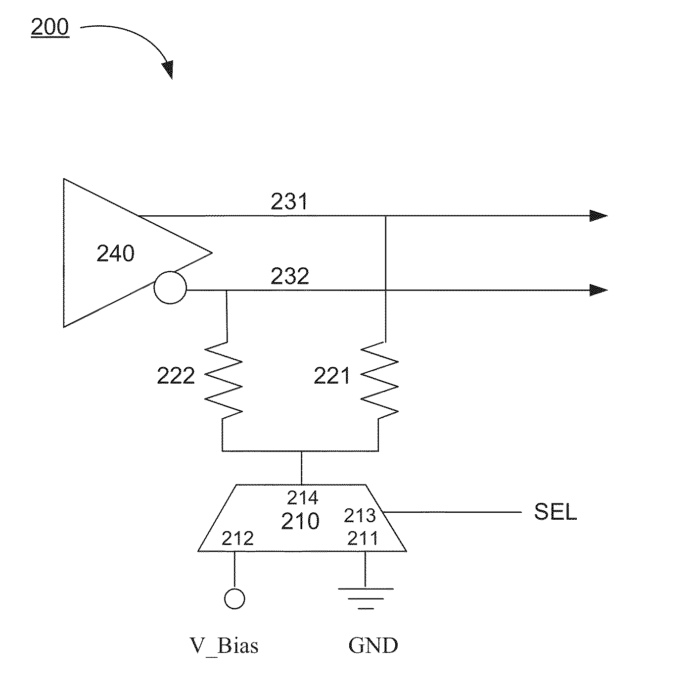
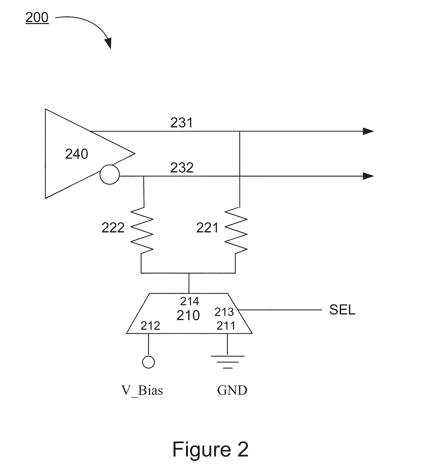
[0044]Example embodiments are described herein in the context of the chip comprising a signal transmitting circuit, the communication system between multiple chips and the method for configuring the communication system between multiple chips. Those of ordinary skill in the art will realize that the following description is illustrative only and is not intended to be in any way limiting. Other embodiments will readily suggest themselves to those skilled in the art having the benefit of this disclosure. Reference will now be made in detail to implementations of the example embodiments as illustrated in the accompanying drawings. The same reference indicators will be used to the extent possible throughout the drawings and the following description to refer to the same or like items.

[0045]Reference will now be made in detail to the preferred embodiments of the present invention, examples of which are illustrated in the accompanying drawings.

[0046]The present invention discloses a chip ...


PUM


Abstract

A chip comprising a signal transmitting circuit, a communication system between multiple chips and a method for configuring the communication system between multiple chips are provided. The signal transmitting circuit of the chip comprises a multi-route selector, a first bias resistor and a second bias resistor, a first signal line and a second signal line, and a signal transmitting end; wherein the multi-route selector comprises a first input end, a second input end, a selection input end and an output end, wherein the first input end is grounded, the second input end is connected to a DC bias voltage and the selection input end receives a selection signal; wherein the multi-route selector selects the first input end when the selection signal is a first selection signal, and the multi-route selector selects the second input end when the selection signal is a second selection signal.

Description

CLAIM OF PRIORITY[0001]The present application claims the priority of Chinese Patent Application No. 201210041881.2, filed Feb. 22, 2012, which is incorporated herein by reference.FIELD OF INVENTION[0002]The present invention relates generally to chip technology field and, in particular, to a chip comprising a signal transmitting circuit, a communication system between multiple chips and a method for configuring the communication system between multiple chips.BACKGROUND[0003]In the prior art, AC coupling capacitors are designed between multiple chips communicating with each other because that: according to PCIE (PCI-Express) standards, a DC bias voltage set at a transmitting end (named as Tx) is V_bias (less than 3.6V), while a DC bias voltage set at a receiving end (named as Rx) is 0V. The difference of the DC bias voltages set at Tx and Rx makes DC common mode voltages of the signals at Tx and Rx different. Further, the different DC common mode voltages of the signals at Tx and Rx...

Claims


Application Information

Patent Timeline
Patent Type & Authority Patents(United States)
IPC IPC(8): H03K19/003
CPCH04L25/0272
Inventor WANG, FEI
Owner NVIDIA CORP
Why Eureka
Try Eureka