Tunable plasmonic filter

a plasmonic filter and plasmonic filter technology, applied in the direction of instrumentation, solid-state device signal generators, picture signal generators, etc., can solve the problems of color quality difficult to control, liquid crystal response time is much slower than that of a typical electronics circuit,

Inactive Publication Date: 2013-06-11
NANOLAMBDA
View PDF24 Cites 45 Cited by
  • Summary
  • Abstract
  • Description
  • Claims
  • Application Information

AI Technical Summary

Problems solved by technology

However, the response time of liquid crystal is much slower than that of a typical electronics circuit.
Because of the spectral broadness and spectral irregular shape of the filter, the color quality is hard to control.

Method used


Image

  • Tunable plasmonic filter
  • Tunable plasmonic filter
  • Tunable plasmonic filter

Examples


first embodiment

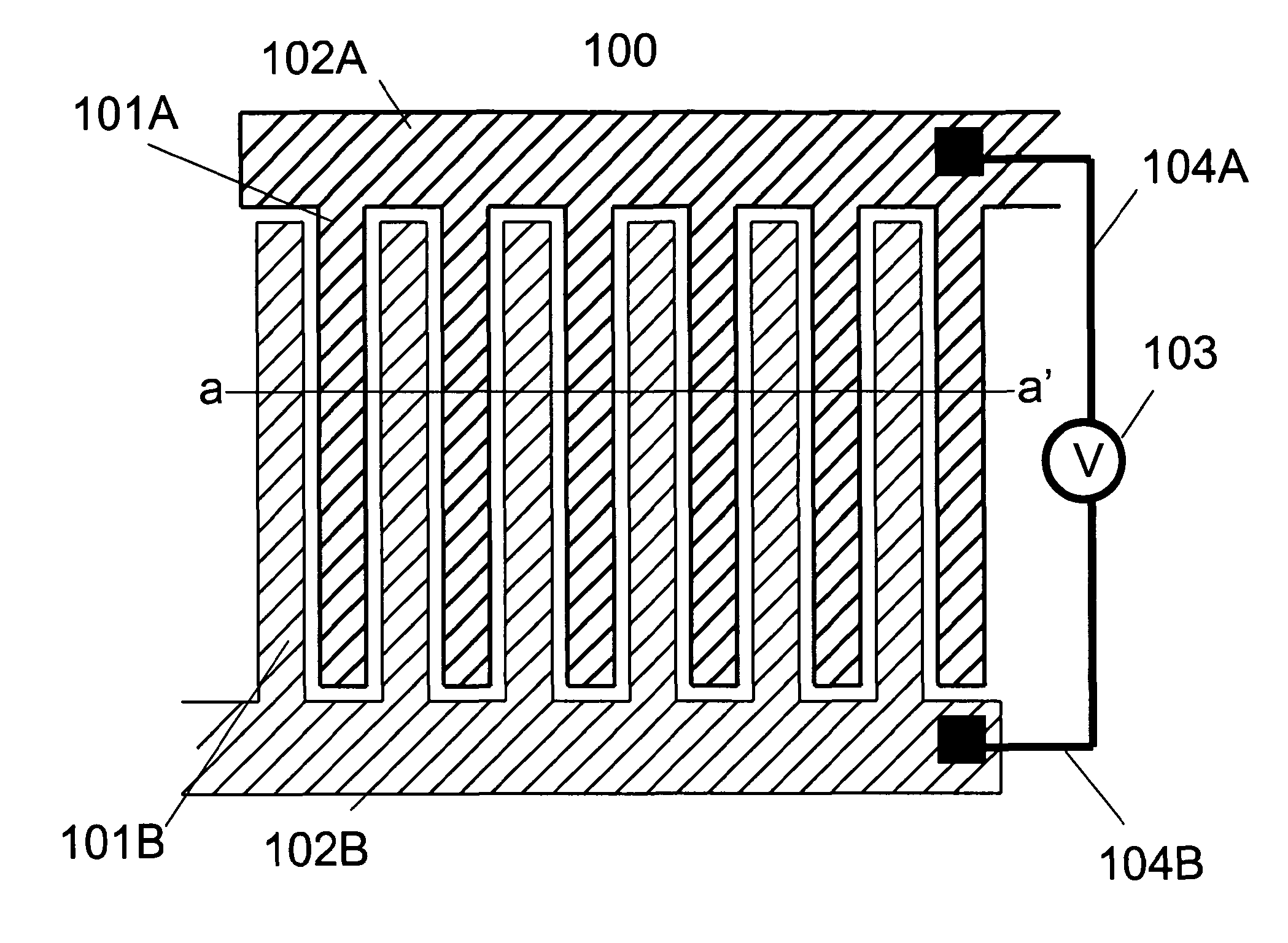
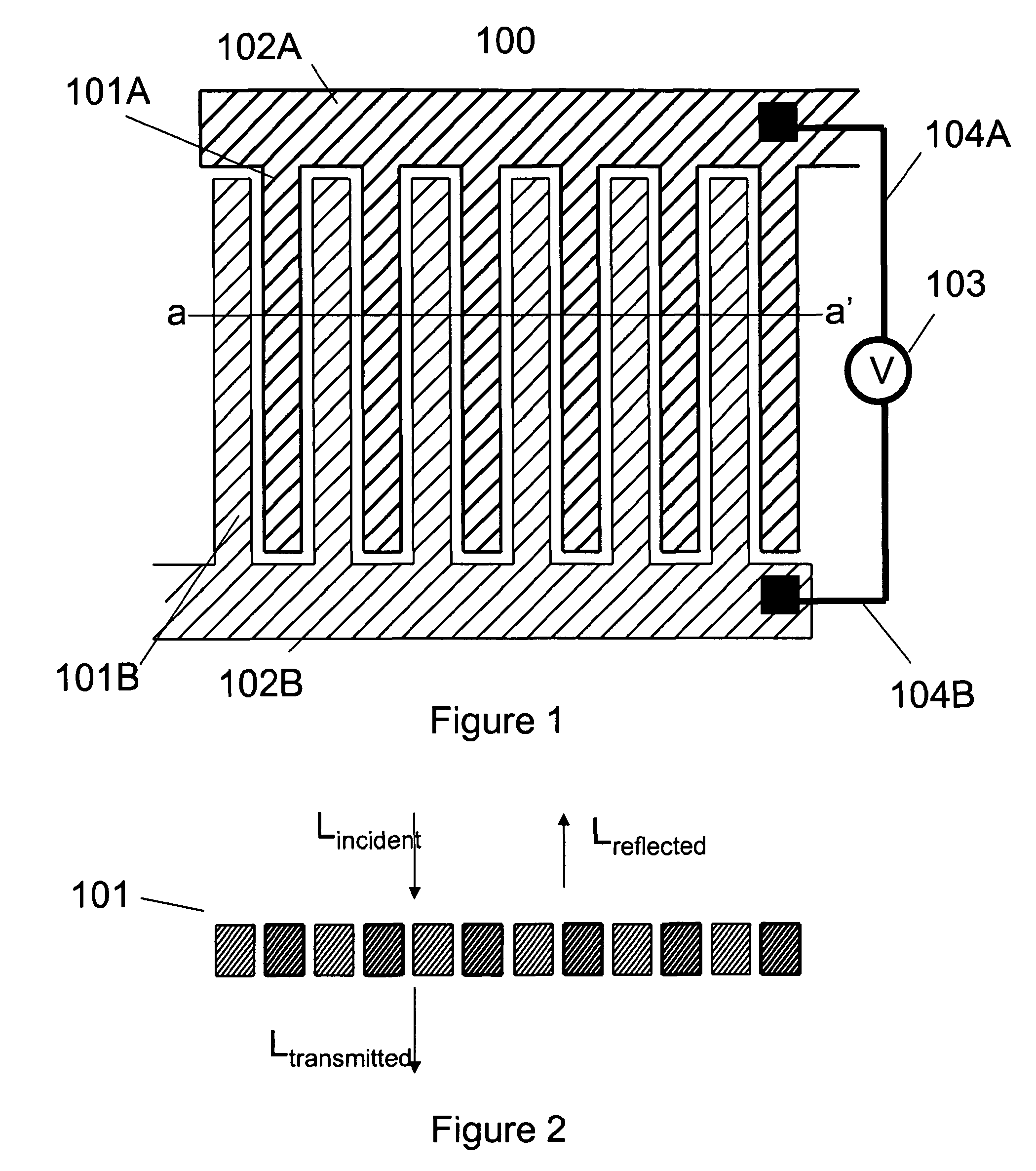
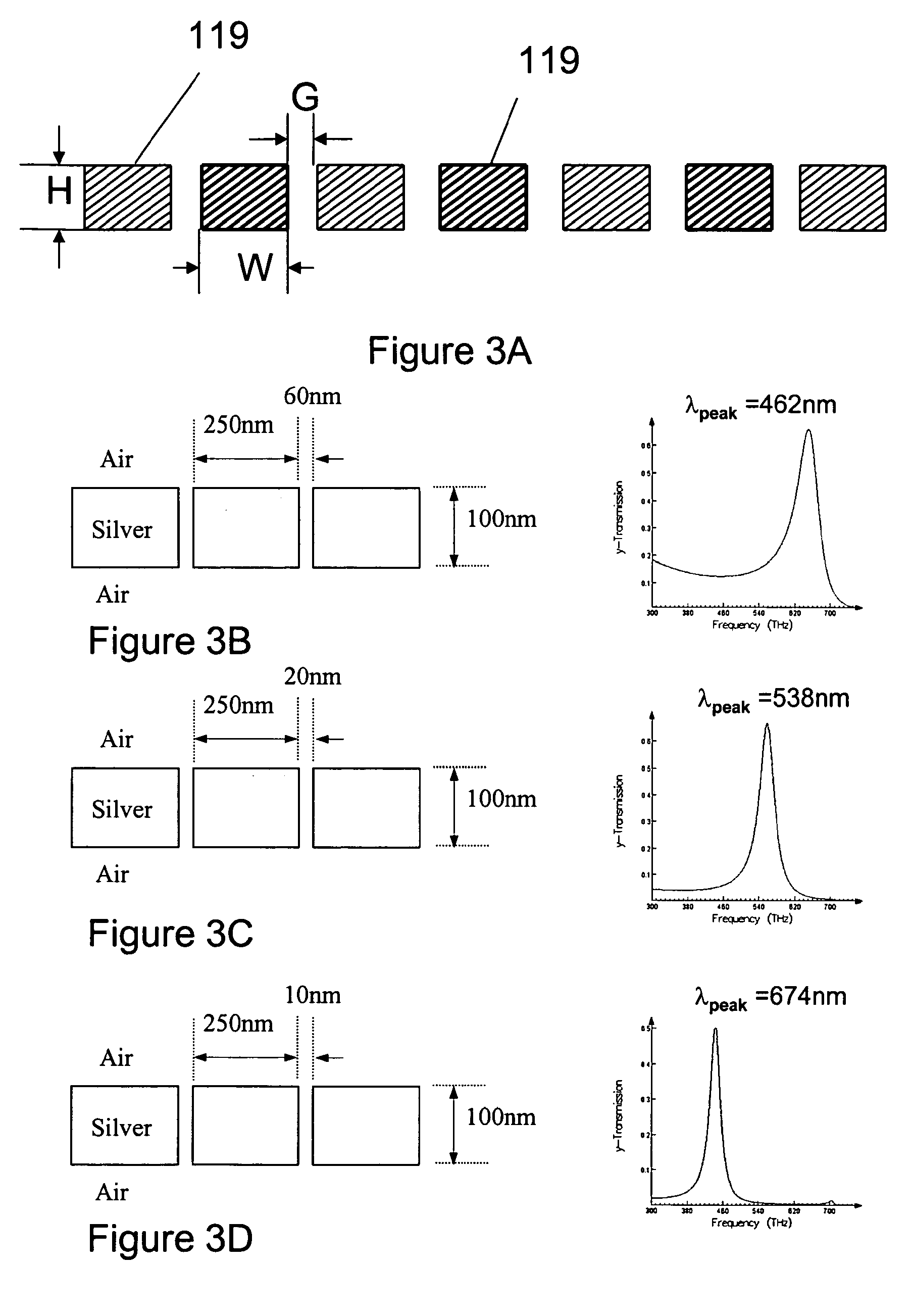
[0020]FIG. 1 illustrates the invention in which a control voltage or current is applied between portions of the metal plasmonic filter. In FIG. 1, a plasmonic tunable filter 100 contains interdigitated metal island or finger structures 101, such as subwavelength island structures separated from each other by subwavelength gaps. The first set of islands or fingers 101A are electrically connected together by a metal connector 102A. The second set of islands or fingers 101B are electrically connected together by a metal connector 102B. The metal may be any metal and is preferably Ag, Au, Cr or Al or alloys thereof. A voltage or current source 103 is connected to each set of islands or fingers via separate leads 104A and 104B. Thus, one output of the voltage or current source is connected to the first part 101A / 102A of interdigitated plasmonic filter structure and the other output is connected to the second part 101B / 102B of the interdigitated plasmonic filter structure. The voltage or ...

second embodiment

[0026]FIG. 4A illustrates an alternative configuration of tunable plasmonic filter according to the invention, in which a control voltage or current is applied indirectly to the metal plasmonic filter structure array. In this configuration, the voltage is applied from a voltage source 403 to electrically conductive electrodes, such as plates 401, 402 located adjacent to the plasmonic metal filter structure array 101. For example, the plates 401, 402 may be located on the opposite sides of the array 101 and be connected to opposite polarity outputs of the voltage source 403.

[0027]For display applications, one or both plates 401 and 402 may comprise optically transparent and electrically conductive plates. For example, the plates may comprise a transparent, conductive material, such as indium tin oxide or aluminum zinc oxide, or a composite material comprising an insulating transparent matrix, such as a polymer matrix, and an electrically conductive filler, such as metal wires or carb...


PUM

PropertyMeasurementUnit
widthaaaaaaaaaa
widthaaaaaaaaaa
heightaaaaaaaaaa

Abstract

A tunable plasmonic filter or an optical filtering method discloses plasmonic filter structure and a voltage or current source. An intensity or wavelength of light transmitted through the filter structure is modulated by the intensity of a voltage or current from the voltage or current source. The plasmonic filter structure is located between electrodes electrically connected to the voltage or current source. The plasmonic filter structure is configured such that the incident light is resonant with at least one plasmonic mode on the structure, and a predetermined wavelength will perturb the metallic plasmonic structure in surface plasmon on energy bands for the wavelength selective transmission of light.

Description

CROSS-REFERENCE TO RELATED PATENT APPLICATIONS[0001]The present application is a National Stage of PCT / US2007 / 026069, filed Dec. 21, 2007, which claims benefit of U.S. provisional application 60 / 877,644, filed Dec. 29, 2006, which are incorporated herein by reference in their entirety.BACKGROUND OF THE INVENTION[0002]Optical filtering is an important concept in optics, and is commonly involved in a variety of optical components and instruments. One example is to use optical filters for a flat panel display. A flat panel display uses a light source, a tunable optical switch and a color filter. Liquid crystal is typically used to modulate the intensity of the light through a pixel. However, the response time of liquid crystal is much slower than that of a typical electronics circuit. And color filters are also used to select a specific spectral range for the pixel. Because of the spectral broadness and spectral irregular shape of the filter, the color quality is hard to control. There...

Claims


Application Information

Patent Timeline
Patent Type & Authority Patents(United States)
IPC IPC(8): G02F1/01G02F1/19
CPCG02F1/19H04N9/045G02F1/01G02F2201/123G02F2201/124G02F2203/10
Inventor LEE, BYOUNGHEECHOI, BYUNG IL
Owner NANOLAMBDA
Why Eureka
Try Eureka