Donor substrate for laser induced thermal imaging and method of fabricating organic light emitting diode using the same

a technology of laser induced thermal imaging and donor substrate, which is applied in the direction of thermography, printing, other printing apparatuses, etc., can solve the problems of deterioration of luminous efficiency and lifetime, difficult manufacture and difficult manufacturing of perfect full color displays

Active Publication Date: 2013-07-16
SAMSUNG DISPLAY CO LTD
View PDF9 Cites 81 Cited by
  • Summary
  • Abstract
  • Description
  • Claims
  • Application Information

AI Technical Summary

Benefits of technology

[0012]The present invention provides a donor substrate for laser induced thermal imaging (LITI) and a method of fabricating an organic light emitting diode (OLED) using the same, which can prevent a transferred emission layer from being damaged by heat so that no wrinkles are formed on the surface of the emission layer, and which can control the difference in transfer characteristics according to the kind of material used to form the emission layer so that it is possible to select various materials used to form the emission layer.
[0013]In the present invention, the damage is prevented by forming a first transfer layer or a buffer layer between an emission layer and a light-to-heat conversion layer. The first transfer layer or the buffer layer is formed of an organic layer, an inorganic layer, or a double layer thereof. The first transfer layer or the buffer layer has an absolute value of lowest unoccupied molecular orbital (LUMO) energy level of 2.6 eV to 3.0 eV and a band gap energy of 2.8 eV to 3.4 eV. Moreover, because the difference in transfer characteristics depending on the kind of material used to form the emission layer is controlled by the first transfer layer or the buffer layer, it is possible to select various materials used to form the emission layer.

Problems solved by technology

However, in the case of vacuum deposition, there is a difficulty in forming the organic layer into a highly precise pattern, and thus manufacture of a perfect full color display is difficult.
Moreover, in the case of photolithography, there is a problem in that the organic layer may be damaged by a developing solution or an etching solution, which results in deterioration of luminous efficiency and lifetime.
In this case, there is a problem in that the emission layer included in the transfer layer is damaged by heat and thus wrinkles are formed on the surface of the transferred emission layer, and interface characteristics deteriorate.
Moreover, there is a problem in that, since transfer characteristics vary according to the kind of material used to form the emission layer, the thickness or properties of the emission layer may be changed after transfer, even if the same laser beam is applied.

Method used


Image

  • Donor substrate for laser induced thermal imaging and method of fabricating organic light emitting diode using the same
  • Donor substrate for laser induced thermal imaging and method of fabricating organic light emitting diode using the same
  • Donor substrate for laser induced thermal imaging and method of fabricating organic light emitting diode using the same

Examples


experimental example

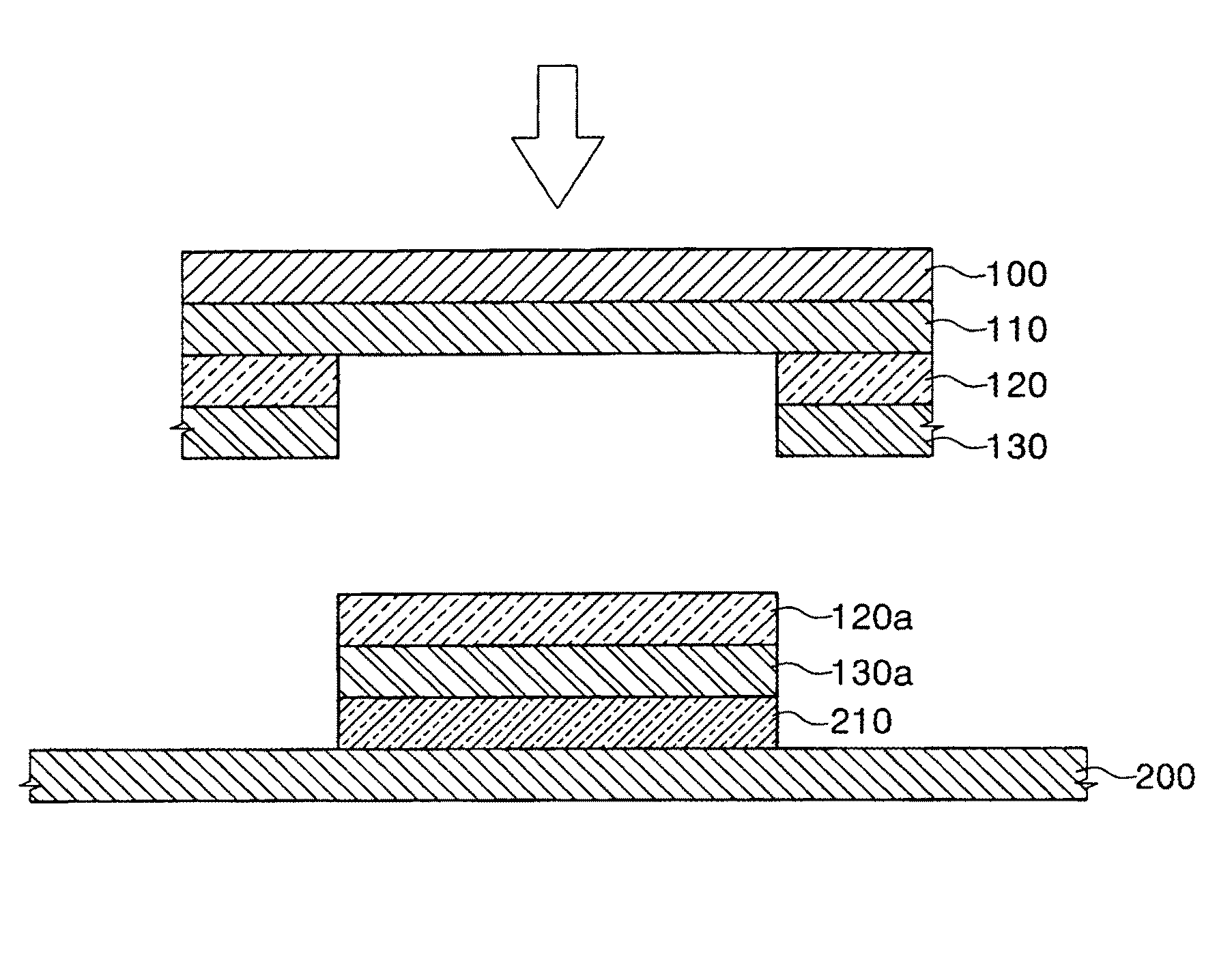
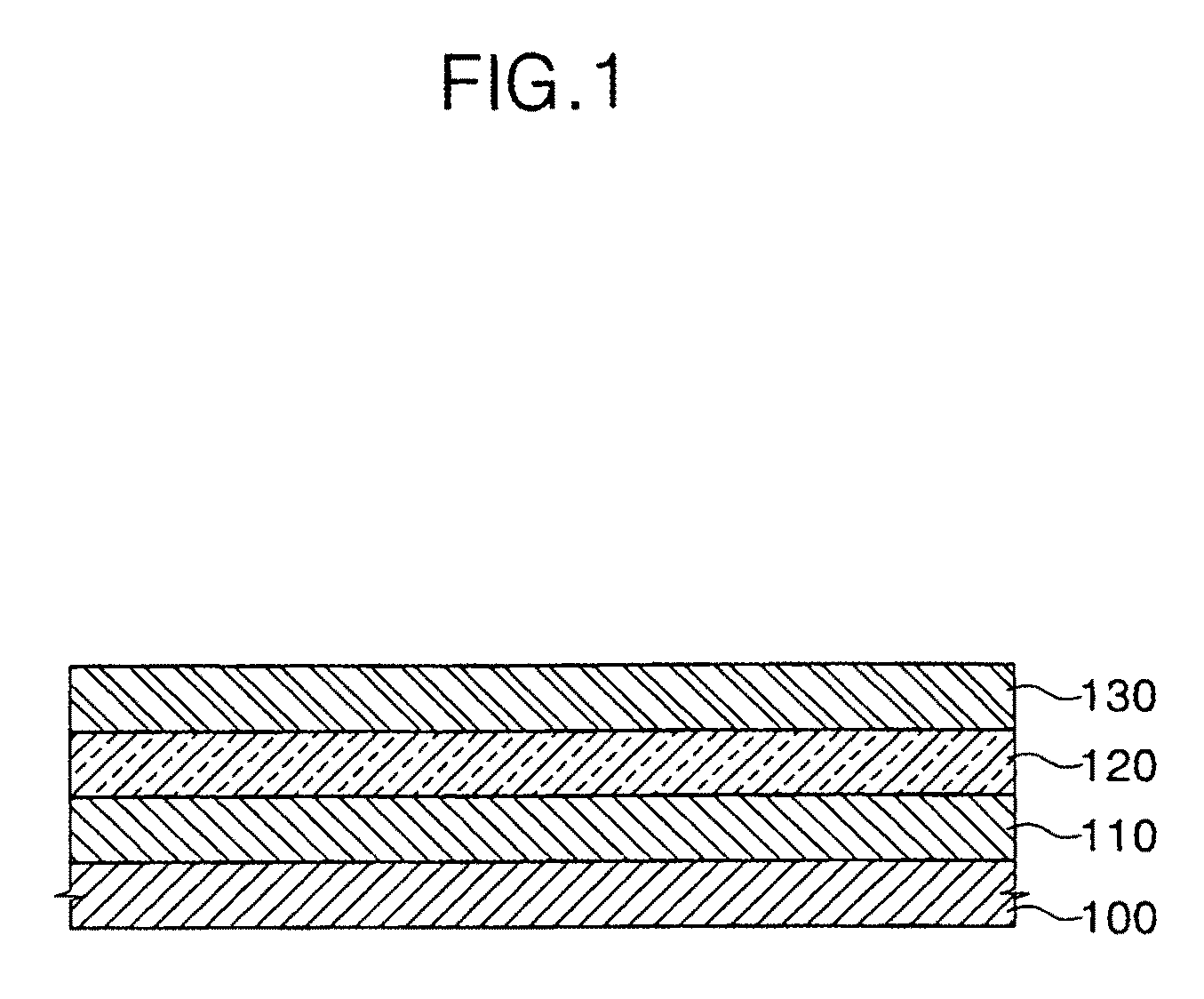
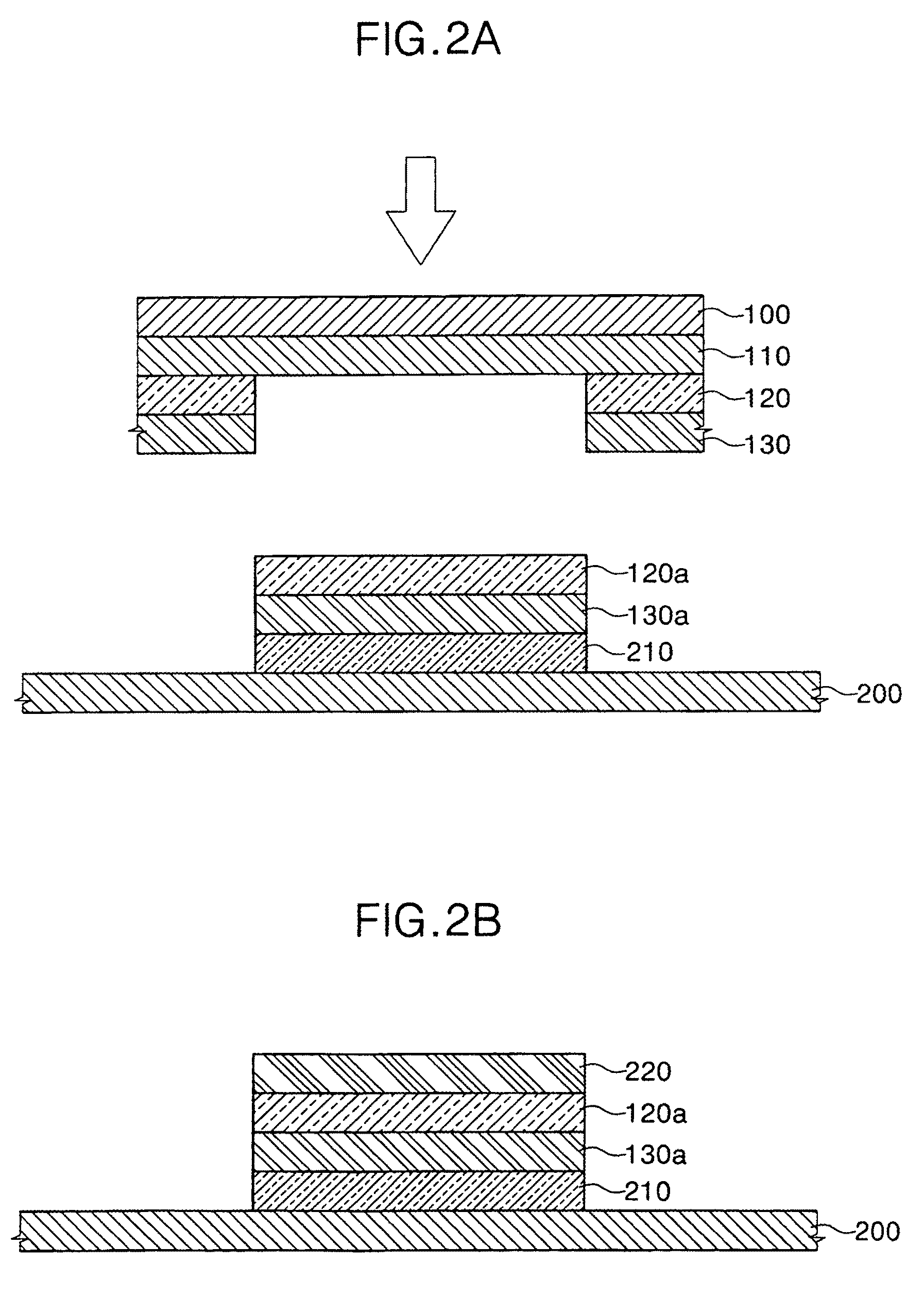
[0054]A base layer was formed of polyethylene terephthalate, and a light-to-heat conversion layer including carbon black as a light absorbing material was formed on the base layer. A first transfer layer was formed of TC1558 (manufactured by Tetrahedron, LUMO: 2.93 eV; band gap energy: 2.96 eV) to a thickness of 50 Å on the light-to-heat conversion layer. A green emission layer including GGH01 (manufactured by Gracel) as a host material and GGD01 (manufactured by Gracel) as a dopant material was formed to a thickness of 200 Å on the light-to-heat conversion layer. A first hole transport layer was formed of NPB to a thickness of 300 Å on the green emission layer, thus preparing a donor substrate including a second transfer layer having the emission layer.

[0055]A first electrode was formed of ITO on a glass substrate, and a hole injection layer was formed of IDE-406 (manufactured by Idemitsu) on the first electrode. Subsequently, a second hole transport layer was formed of NPB on the ...


PUM

PropertyMeasurementUnit
band gap energyaaaaaaaaaa

Abstract

Provided are a donor substrate for laser induced thermal imaging (LITI) and a method of fabricating an organic light emitting diode (OLED) using the same, which can prevent a transferred emission layer from being damaged by heat and thus prevent wrinkles from forming on the surface thereof. The donor substrate includes a base layer, a light-to-heat conversion layer disposed on the base layer, a first transfer layer disposed on the light-to-heat conversion layer and including an organic layer, an inorganic layer, or a double layer thereof, and a second transfer layer disposed on the first transfer layer and including an emission layer. The first transfer layer has an absolute value of lowest unoccupied molecular orbital energy level of 2.6 to 3.0 eV and a band gap energy of 2.8 to 3.4 eV.

Description

CLAIM OF PRIORITY[0001]This application makes reference to, incorporates the same herein, and claims all benefits accruing under 35 U.S.C. §119 from an application earlier filed in the Korean Intellectual Property Office on 26 Aug. 2008 and there duly assigned Serial No. 10-2008-0083345.BACKGROUND OF THE INVENTION[0002]1. Field of the Invention[0003]The present invention relates to a donor substrate for laser induced thermal imaging (LITI) and a method of fabricating an organic light emitting diode (OLED) using the same, and more particularly, to a donor substrate for laser induced thermal imaging (LITI) and a method of fabricating an OLED using the same. The OLED and the method of fabricating the OLED of the present invention prevent a transferred emission layer from being damaged by heat and thus prevent wrinkles from forming on the surface thereof.[0004]2. Description of Related Art[0005]Among flat panel displays (FPDs), an organic light emitting diode (OLED) display has the adva...

Claims


Application Information

Patent Timeline
Patent Type & Authority Patents(United States)
IPC IPC(8): B41M5/34
CPCB41M5/38214B41M5/42H01L51/0013B41M5/38228B41M5/385B41M2205/38Y02E10/549H10K71/18H05B33/10H10K71/00
Inventor LEE, SEUNG-MOOKPARK, JIN-WOOPYO, SANG-WOOJUNG, MYUNG-JONGKIM, DO-YOUNGKIM, DAE-HOONKIM, HYO-YEON
Owner SAMSUNG DISPLAY CO LTD
Why Eureka
Try Eureka