Inkjet head

a technology of inkjet and ink chamber, applied in printing and other directions, can solve the problems of difficult formation of thick layers, high density individual ink chambers, voltage drop especially near the center, etc., and achieve the effect of reducing resistance, uniform discharging of ink, and reducing variance in mechanical compliance of ink channels

Active Publication Date: 2013-07-23
RICOH KK
View PDF19 Cites 2 Cited by
  • Summary
  • Abstract
  • Description
  • Claims
  • Application Information

AI Technical Summary

Benefits of technology

[0020]The present invention is made in light of the above problems, and provides an inkjet head of a smaller size in which uniform discharging of ink is improved by lowering the resistance of a common electrode interconnect to reduce variance in mechanical compliance of ink channels even when the number of nozzles is large.

Problems solved by technology

For the type using an actuator, although it is capable to use ink of a wide variety of physical properties, there has been a problem in making high density individual ink chambers for downsizing a head.
When forming electrodes or interconnects by the thin layer forming technique, as a layer of a metal or an alloy is formed by sputtering, Chemical Vapor Deposition (CVD), or the like it is difficult to form a thick layer.
However, when the resistance of the common electrode interconnect is high, voltage drop occurs especially near the center.
For nozzles near the center, since not enough voltage is applied to the corresponding piezoelectric elements, droplets cannot be properly discharged which deteriorates uniform discharging.
Therefore, there is a problem that the high density of nozzles obtained by the semiconductor device manufacturing process cannot be utilized because of the high resistance of the common electrode interconnect.
When the common electrode interconnect is as thin as such, it is necessary to have the dimension of the common electrode interconnect larger which results in a larger size of an inkjet head.
When forming a thicker layer, it may be difficult to form a layer having a uniform thickness.
When the layer is not uniform, it is difficult to bond another substrate or the like to the layer.
Therefore, if the common electrode interconnect is not flat, the substrate cannot be properly bonded.

Method used


Image

  • Inkjet head
  • Inkjet head
  • Inkjet head

Examples


example 1

RELATIVE EXAMPLE 1

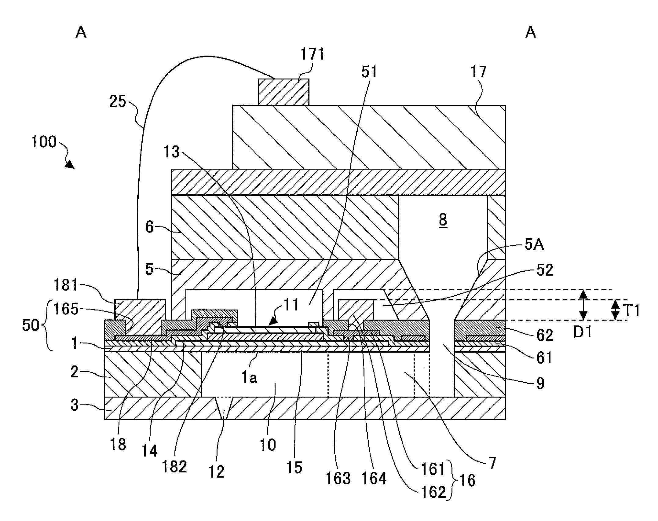
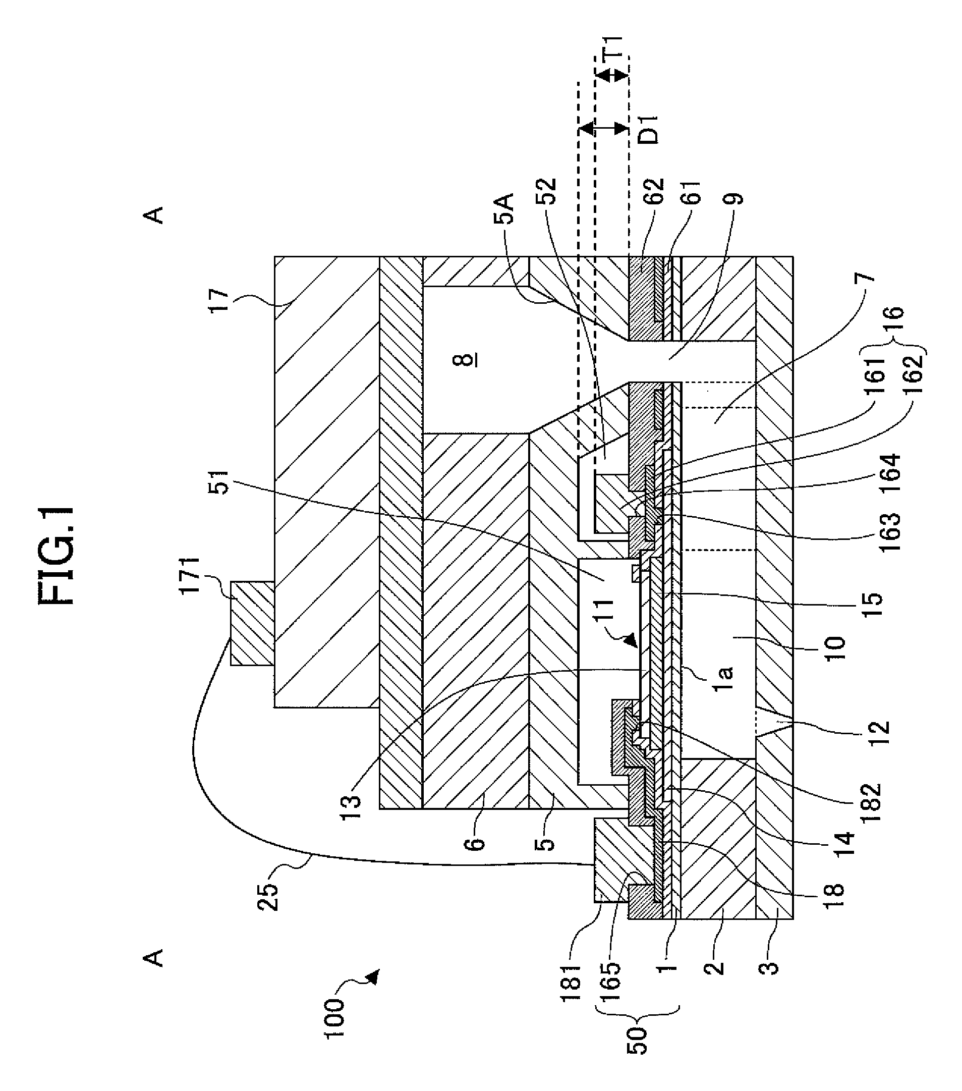
[0128]In this relative example, an inkjet head was formed in accordance with a similar method as example 1. However, in this relative example, the second common electrode interconnect 162 was not formed.

[0129]Then, the drop speed of the discharged ink was measured by the flash camera similarly as example 1.

[0130]As a result, an average drop speed of the discharged ink of all of the piezoelectric element 11 was lowered to 6.8 m / s. Further, the variance in the drop speed between the piezoelectric element 11 closest to the common electrode pad 191 and the piezoelectric element 11 farthest (for 300 pitch) from the common electrode pad 191 was ±15%. Further, the variance in the drop speed when the adjacent piezoelectric element 11 is actuated became larger (about 10%) than that of example 1.

[0131]It means that the resistance of the common electrode interconnect 16 cannot be lowered enough so that a voltage drop was generated. Further, the function of the vibration layer...

example 2

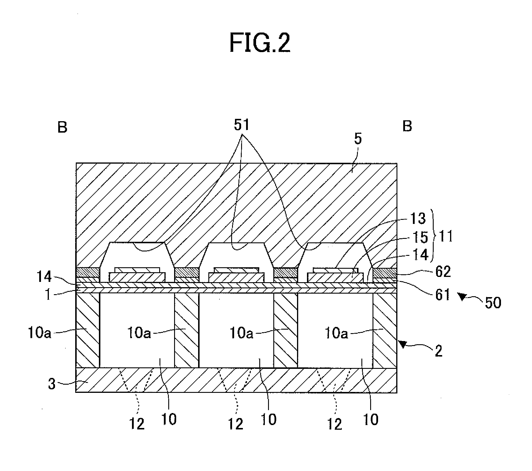
[0132]In this example, an inkjet head 100 was formed in accordance with a similar method as example 1. However, in this example, the insulating interlayer 62 was formed between the first common electrode interconnect 161 and the second common electrode interconnect 162.

[0133]After patterning the individual electrode interconnects 18 and the first common electrode interconnect 161, Si3N4 (2 μm thickness) was formed as the insulating interlayer 62 by plasma CVD. Then, the contact holes 164 in which contacts for electrically connecting the second common electrode interconnect 162 and the first common electrode interconnect 161 and the contact holes 165 in which contacts for connecting the common electrode pads 191 and the first common electrode interconnect 161, and the individual electrode pads 181 and the individual electrode interconnects 18 are formed were formed in the insulating interlayer 62 by dry-etching.

[0134]Then, by forming a Ni layer (20 μm thickness) on the insulating int...


PUM


Abstract

Disclosed is an inkjet head including a channel substrate; a multi-interconnect structure formed on the channel substrate, including a vibration layer, plural piezoelectric elements each including a first electrode, a piezoelectric layer and a second electrode, and a common electrode interconnect electrically connected to the first electrode including a first common electrode interconnect and a second common electrode interconnect which has a thickness thicker than that of the first common electrode interconnect; and a support substrate bonded to the channel substrate through the multi-interconnect structure, the support substrate being provided with a first concave portion at a surface facing the channel substrate at an area corresponding to the second common electrode interconnect to accommodate the second common electrode interconnect.

Description

BACKGROUND OF THE INVENTION[0001]1. Field of the Invention[0002]The present invention relates to an inkjet head, and more specifically, to an inkjet head that discharges droplets from micro nozzles in accordance with a pressure change generated by applying electric power to a piezoelectric element provided at an individual ink chamber to form a pattern.[0003]2. Description of the Related Art[0004]For an inkjet head that forms a pattern by discharging micro droplets, plural types of products are provided where a pressure change is generated in an individual ink chamber. For example, there are a thermal inkjet type in which a heater is set in the individual ink chamber to vaporize liquid to cause a pressure change and a type using an actuator set in the individual ink chamber. For the type using an actuator, based on the type of actuators, a piezoelectric element type or an electrostatic type may be included.[0005]For the type using an actuator, although it is capable to use ink of a ...

Claims


Application Information

Patent Timeline
Patent Type & Authority Patents(United States)
IPC IPC(8): B41J2/045B41J2/14
CPCB41J2/161B41J2002/14241B41J2002/14491
Inventor KATO, MASAKIYAMAGUCHI, KIYOSHISHINGYOHUCHI, MITSURU
Owner RICOH KK
Why Eureka
Try Eureka